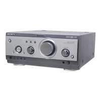
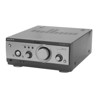
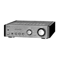
Note on Printed Wiring Boards:
• X : parts extracted from the component side.
• Y : parts extracted from the conductor side.
•
f
: internal component.
• : Pattern from the side which enables seeing.
• Indication of transistor.
Note on Schematic Diagram:
• All capacitors are in µF unless otherwise noted. pF: µµF
50 WV or less are not indicated except for electrolytics
and tantalums.
• All resistors are in Ω and
1
/
4
W or less unless otherwise
specified.
•
f
: internal component.
• 2 : nonflammable resistor.
• 5 : fusible resistor.
• C : panel designation.
• A : B+ Line.
• B : B– Line.
• Voltages are dc with respect to ground under no-signal
conditions.
no mark : Power on
( ) : Output is more than 1 W.
• Voltages are taken with a VOM (Input impedance 10 MΩ).
Voltage variations may be noted due to normal produc-
tion tolerances.
• Signal path.
F : AUDIO
N : MIC
• Abbreviation
AUS : Australian model
EA : Saudi Arabia model
KR : Korean model
MX : Mexican model
SP : Singapore model
TH : Thai model
Note: The components identified by mark 0 or dotted line
with mark 0 are critical for safety.
Replace only with part number specified.
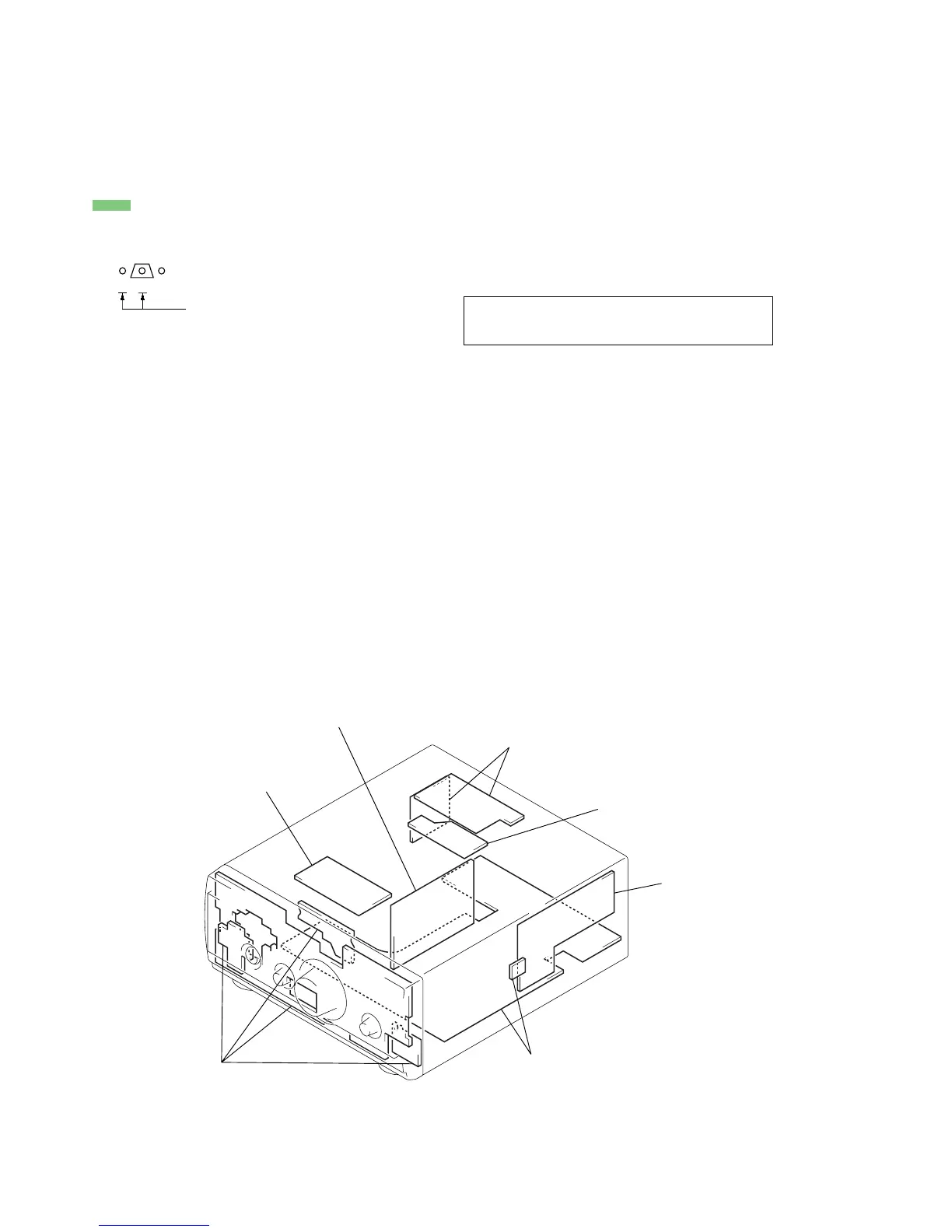
• Circuit Boards Location
AC OUTPUT board
SURROUND AMP board
SUB TRANS board
AC INPUT board
RELAY boar