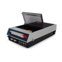
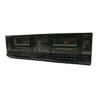
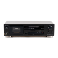
TC-S3
1717
7-5. SCHEMATIC DIAGRAM – LEAF SW Section –
7-6. PRINTED WIRING BOARD – LEAF SW Section – • See page 13 for Circuit Boards Location.
PM901
PM902
A
CN311
IC1001
IC1002
A
B
C
D
1 2 3 4 5 6 7 8 9 10 11 12
(Page 16)
D1001 B-4
D1002 B-10
IC1001 B-2
IC1002 B-9
Q1001 B-3
• Semiconductor
Location
Ref. No. Location
C1001
33
10V
S1004
(A. 120/70)
S1008
(B. 120/70)
A
MAIN BOARD
(2/2)
CN311
There are a few cases that the part printed on
this diagram isn’t mounted in this model.
• Voltages are dc with respect to ground under no-signal
conditions.
no mark : TAPE PLAY
( ) : TAPE REC
(Page 15)
 Loading...