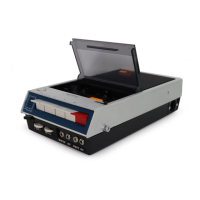
19
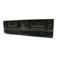
TC-S3
7-9. IC PIN FUNCTION DESCRIPTION
• MAIN BOARD IC310 PT8300-S (SYSTEM CONTROL)
Pin No. Pin Name I/O Description
1 VSS —
Ground terminal
2 RESET_B I
Reset signal input terminal Not used
3 CLK I
Serial data transfer clock signal input from the CD player section (CDP-S3)
4 LATCH I
Serial data latch pulse signal input from the CD palyer section (CDP-S3)
5 – 8 P15 – P12 I
Not used (fixed at “L”)
9 P11 I
AMS signal input terminal “L”: AMS in
10 P10 I
Detection input from the deck-A half detect switch “H”: cassette in, “L”: no cassette
11 P9 I
Detection input from the deck-B play detect switch “H”: deck-B play
12 P8 I
Detection input from the deck-A play detect switch “H”: deck-A play
13 LATCHO O
Serial data latch pulse output to the PT8300-S (IC311)
14 CLKO O
Serial data transfer clock signal output to the PT8300-S (IC311)
15 DO1 O
Serial data output to the PT8300-S (IC311)
16 DI2 I
Serial data input from the PT8300-S (IC311)
17 P7 O
Tape deck relay on/off control signal output to the µPC1330H (IC302)
18 P6 O
ALC on/off control signal output to the HA12226F (IC301)
19 P5 O
Deck-A/B selection signal output to the HA12226F (IC301)
20 P4 O
EQ high/normal selection signal output to the HA12226F (IC301)
21 P3 O
Recording bias on/off control signal output to the HA12226F (IC301)
22 P2 O
Recording muting on/off control signal output to the HA12226F (IC301)
23 P1 O
Dolby NR on/off selection signal output to the HA12226F (IC301)
24 P0 O
Tape deck line muting on/off control output to the HA12226F (IC301)
25 DO2 O
Serial data output to the CD player section (CDP-S3)
26 DI1 I
Serial data input from the CD player section (CDP-S3)
27 PULLUP I
P8 to P15 Control pin for pull-up resisitor (fixed at “L”)
28 VCC —
Power supply terminal (+5V)
 Loading...