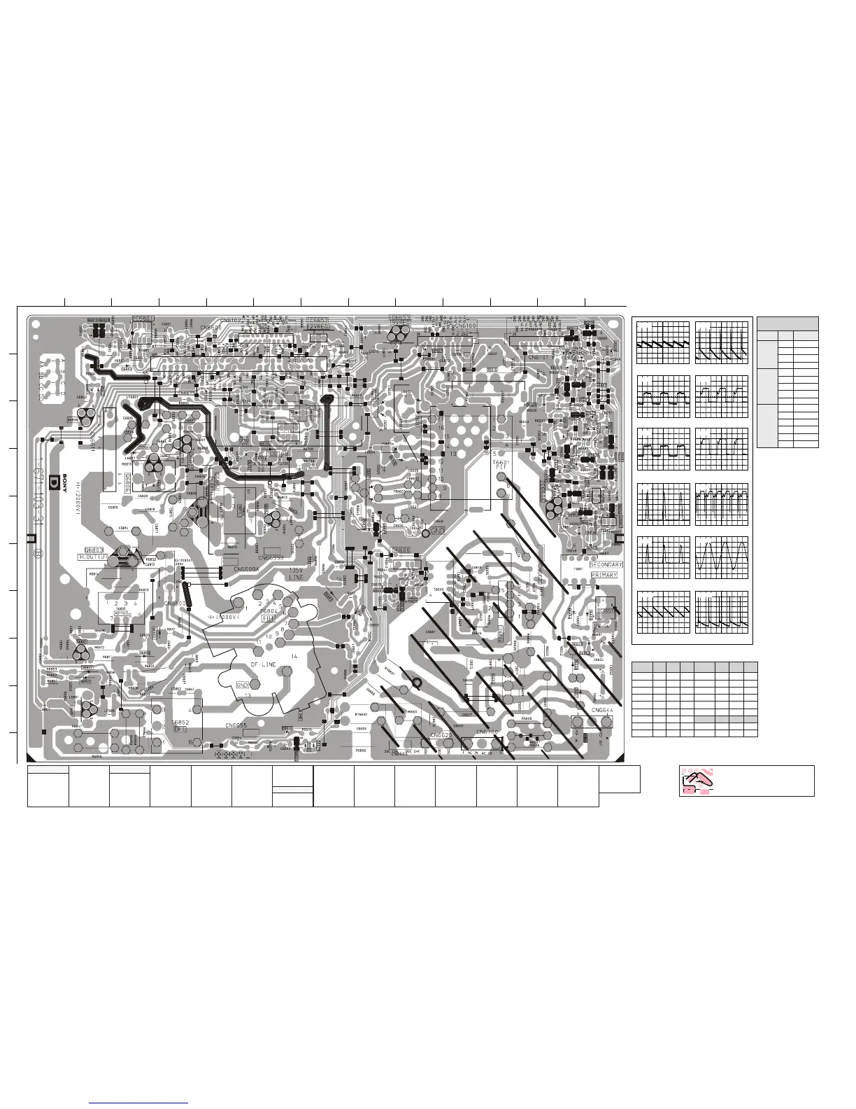
NOTE:
Portions of the circuit marked as shown are high
voltage areas. Use care to prevent electric shock
during inspection or repair.
6261
D [ PRINTED WIRING BOARD ]
Semiconductor Voltage Table
CI
4566CI5-L
SROTSISNART
7066Q5-I6766Q4-M0076Q3-G6086Q4-C2066D01-F5166D3-M1266D2-L7266D1-J2566D8-M9566D6-M1076D3-G0186D4-D
0066CI6-I7666CI5-N0066Q01-G8066Q2-L7766Q4-N1086Q8-B7086Q2-M3066D4-L6166D4-I2266D3-M8266D1-N3566D8-M6766D3-M5086D8-C1186D4-D
4066CI8-K6766CI5-M2066Q7-I1166Q1-M8766Q4-M2086Q5-F1586Q9-B4066D9-K7166D4-H3266D5-H9266D3-L4566D7-M7766D3-M6086D8-C1586D8-B
1566CI7-M0076CI4-F3066Q7-H1566Q5-M9766Q3-M3086Q6-B
EDOID
5066D5-M8166D2-K4266D2-M0366D2-L5566D7-M8766D3-M7086D7-G2586D8-B
2566CI1-G1086CI1-C5066Q4-L2566Q5-N0866Q3-M4086Q4-E0066D01-G0166D3-M9166D3-H5266D2-M1366D01-F6566D5-M9766D4-M8086D7-H
3566CI1-I6066Q1-M7666Q5-M1866Q4-M5086Q4-D1066D01-G3166D4-M0266D3-I6266D2-M1566D8-M8566D8-M1866D5-M9086D2-M
5ms/div 5ms/div
10us/div 10us/div
10us/div 20us/div
10us/div 10us/div
10us/div 10us/div
5ms/div
5ms/div
570 mVp-p (V) 58 Vp-p (V)
2.28 Vp-p (H)
2.14 Vp-p (H) 150 Vp-p (H)
TP1 TP2
TP3
TP4
D board Waveforms
1.07 kVp-p (H)
131 Vp-p (H)
TP4
TP5 TP6
TP7
2.3 Vp-p (H)
TP8
1.72 kVp-p (H) 265 Vp-p (H)
TP9
TP10
1.98 Vp-p (V) 116 Vp-p (V)
TP11
TP12
feR )e( )b( )c( feR )e( )b( )c(
6766Q8.15.25 3066Q008.11
7766Q8.11.25 5066Q07.00
8766Q8.16.15 8066Q005.3
7086Q04.60 1866Q04.110
1086Q03.0167066Q3.05.05
2086Q04.0-7.371586Q01-6.48
3086Q02.5310
feR )s( )g( )d(
4086Q006.5315086Q0222
2066Q1.98.110 6086Q04.17.531
elbaTegatloVCI
oNfeR
oNniP )V(egatloV
0066CI
17.431
25.2
31.9
40
0076CI
14.1
32.21-
58.0-
60.51
74.1
1086CI
10
20
30
52.2
67.6
71.0
ABCDEF
G
HIJKLM
1
2
3
4
5
6
7
8
9
10
 Loading...