EasyManua.ls Logo

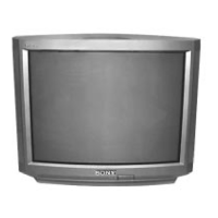
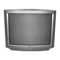
Sony TRINITRON KV-32S12 - Circuit Boards Location

Sony TRINITRON KV-32S12
69 pages
Print Icon
To Next Page IconTo Next Page
To Previous Page IconTo Previous Page
Loading...
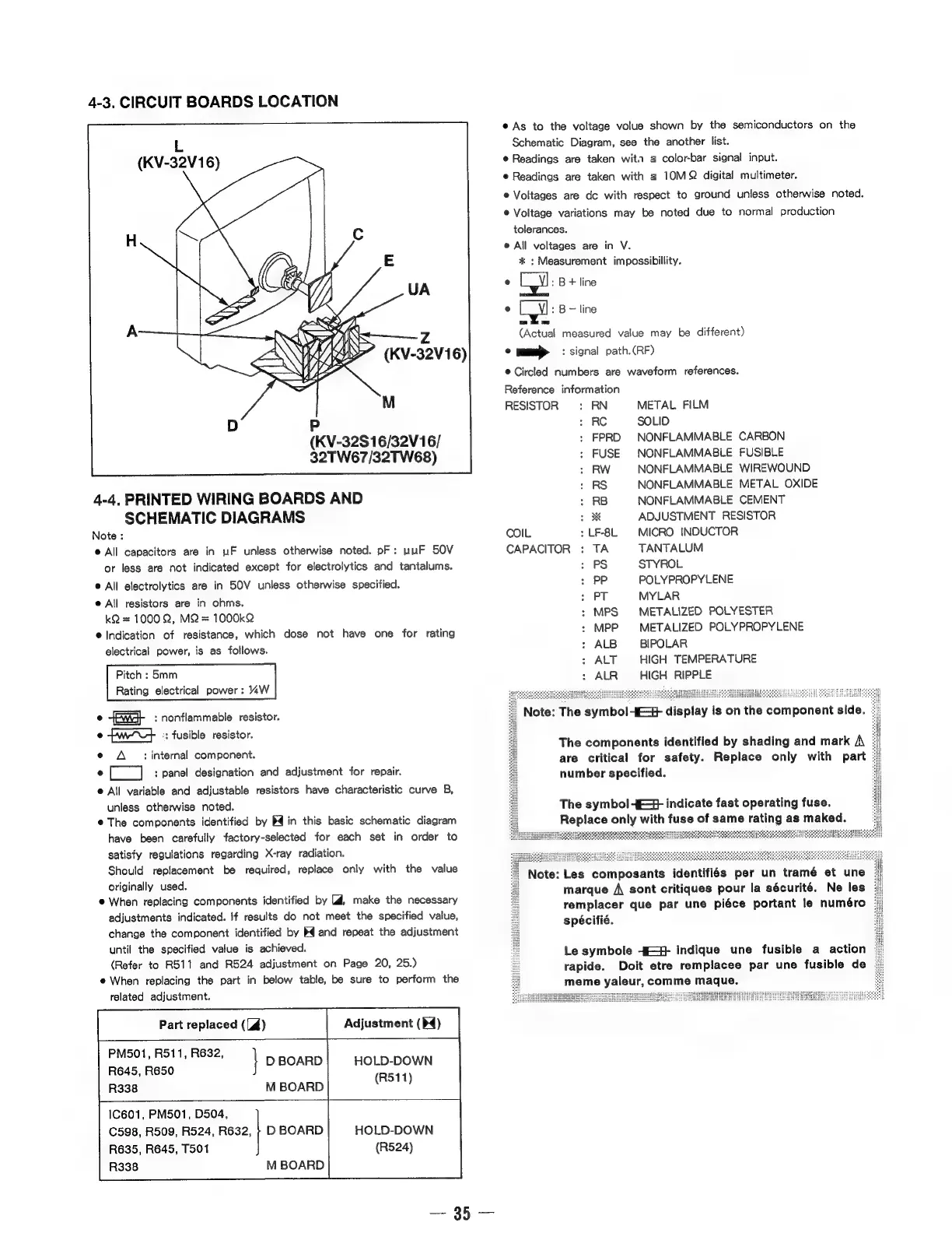
4-3.
CIRCUIT
BOARDS
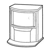
LOCATION
L
(KV-32V1
(KV-32$16/32V16/
32TW67/32TW68)
4-4.
PRINTED
WIRING
BOARDS
AND
SCHEMATIC
DIAGRAMS
Note
:
©
All
capacitors
are
in
uF
unless
otherwise
noted.
pF:
wuF
SOV
or
less
are
not
indicated
except
for
electrolytics
and
tantalums.
e
All
electrolytics
are
in
50V
unless
otherwise
specified.
e
All
resistors
are
in
ohms.
kQ=
1000
2,
MQ
=
1000k2
@
Indication
of
resistance,
which
dose
not
have
one
for
rating
electrical
power,
is
as
follows.
Pitch
:
5mm
Rating
electrical
power:
4%W
©
4B}:
nonflammable
resistor.
e
fw
:
fusible
resistor.
e
A
:internal
component.
°
Cc]
:
panel
designation
and
adjustment
for
repair.
e
All
variable
and
adjustable
resistors
have
characteristic
curve
B,
unless
otherwise
noted.
@
The
components
identified
by
b4
in
this
basic
schematic
diagram
have
been
carefully
factory-selected
for
each
set
in
order
to
satisfy
regulations
regarding
X-ray
radiation.
Should
replacement
be
required,
replace
only
with
the
value
originally
used.
©
When
replacing
components
identified
by
[d,
make
the
necessary
adjustments
indicated.
if
results
do
not
meet
the
specified
value,
change
the
component
identified
by
bd
and
repeat
the
adjustment
until
the
specified
value
is
achieved.
(Refer
to
R511
and
R524
adjustment
on
Page
20,
25.)
e
When
replacing
the
part
in
below
table,
be
sure
to
perform
the
related
adjustment.
Part
replaced
([4)
Adjustment
(P4)
PM501,
R511,
R632,
R645,
R650
}
PPerep
R338
M
BOARD
HOLD-DOWN
(R511)
1C601,
PMS01,
D504,
C598,
R509,
R524,
R632,
;
D
BOARD
R635, R645,
T501
(R524)
R338
M
BOARD
HOLD-DOWN
As
to
the
voltage
volue
shown
by
the
semiconductors
on
the
Schematic
Diagram,
see
the
another
list.
e
Readings
are
taken
wita
a
color-bar
signal
input.
e
Readings
are
taken
with
a
10M
2
digital
multimeter.
e
Voltages
are
de
with
respect
to
ground
unless
otherwise
noted.
@
Voltage
variations
may
be
noted
due
to
normal
production
tolerances.
@
All
voltages
are
in
V.
%*
:
Measurement
impossibillity.
e
Ly):
B
+
tins
e
Lvl:
8
Tine
(Actual
measured
value
may
be
different)
e
a>
:
signal
path.(RF)
©
Circled
numbers
are
waveform
references.
Reference
information
RESISTOR
=:
RN
METAL
FILM
:
RC
SOLID
:
FPRD
NONFLAMMABLE
CARBON
:
FUSE
NONFLAMMABLE
FUSIBLE
:
RW
NONFLAMMABLE
WIREWOUND
:
RS
NONFLAMMABLE
METAL
OXIDE
:
RB
NONFLAMMABLE
CEMENT
2%
ADJUSTMENT
RESISTOR
COIL
:LF-8L
MICRO
INDUCTOR
CAPACITOR
:
TA
TANTALUM
:
PS
STYROL
:
PP
POLYPROPY
LENE
:
PT
MYLAR
:
MPS
METALIZED
POLYESTER
:
MPP
=
METALIZED
POLYPROPYLENE
:
ALB
BIPOLAR
:
ALT
HIGH
TEMPERATURE
ALR
~~
HIGH
RIPPLE
_
Note:
The
symbol
-&=#
display
is
on
the
component
side
The
components
identified
by
shading
and
mark
A\
are
critical
for
safety.
Replace
only
with
part
number
specified.
The
symbol
4&4
indicate
fast
operating
fuse.
Replace
only
with
fuse
of
same
rating
as
maked
:
Les
composants
identifiés
per
un
tramé
et
une
marque
/\
sont
critiques
pour
la
sécurité.
Ne
les
remplacer
que
par
une
piéce
portant
le
numéro
spécifié.
Le
symbole
4+
indique
une
fusible
a
action
rapide.
Doit
etre
remplacee
par
une
fusible
de
meme
yaleur,
comme
maque.

Table of Contents