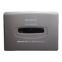
WM-EX190/EX192
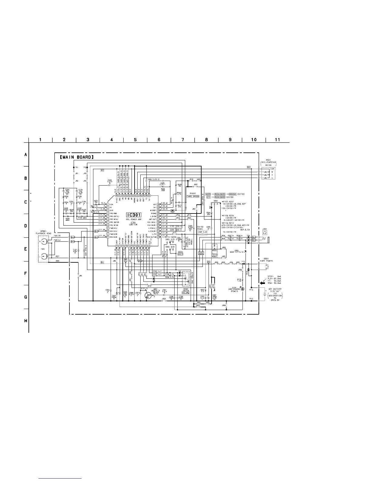
5-3. SCHEMATIC DIAGRAM
— 11 — — 12 —
Note on Schematic Diagram:
• All capacitors are in µF unless otherwise noted. pF: µµF
50 WV or less are not indicated except for electrolytics
and tantalums.
• All resistors are in Ω and
1
/
4
W or less unless otherwise
specified.
• % : indicates tolerance.
• C : panel designation.
• U : B+ Line.
• H : adjustment for repair.
• Total current is measured with no cassette installed.
• Power voltage is dc V and fed with regulated dc power
supply from external power voltage jack.
• Voltages and waveforms are dc with respect to ground
under no-signal (detuned) conditions.
no mark : STOP
( ) :PLAY
• Voltages are taken with a VOM (Input impedance 10 MΩ).
Voltage variations may be noted due to normal produc-
tion tolerances.
• Signal path.
E : PB
• Abbreviation
CND : Canadian model
FR : French model
EA : Saudi Arabia model
• Refer to page 13 for IC Block Diagram.
68
15
15
EX190 : E/
EX192 : AEP, E, EA
2.2M
C609
1000p
C343
1000p
R106, R206
150 : EX192: FR
100 : EXCEPT EX192: FR
R104, R204
680 : EX192: FR
470 : EXCEPT EX192: FR

 Loading...