– 18 – – 20 –– 19 –
r
WAVEFORM
1
IC701 %•
VOLT/DIV : 0.2V AC
TIME/DIV : 5 µsec
1.1Vp-p
75kHz
13.6
µ
sec
r
IC BLOCK DIAGRAM
2
3
5
4
1
+
–
+
–
OUT
VCC
NC
SUB
GND
CO1
OP1
IC702 PST9018NL
Note:
• All capacitors are in µF unless otherwise noted. pF: µµF
50 WV or less are not indicated except for electrolytics
and tantalums.
• All resistors are in Ω and
1
/
4
W or less unless otherwise
specified.
• C : panel designation.
• U : B+ Line.
• Power voltage is dc 3 V and fed with regulated dc power
supply from battery terminal.
• Voltages and waveforms are dc with respect to ground
under no-signal (detuned) conditions.
• Voltages and waveforms are dc with respect to ground in
playback mode.
no mark : FM (RADIO SECTION)
PLAY (TAPE SECTION)
( ) : AM
• Voltages are taken with a VOM (Input impedance 10 MΩ).
Voltage variations may be noted due to normal produc-
tion tolerances.
• Waveforms are taken with a oscilloscope.
Voltage variations may be noted due to normal produc-
tion tolerances.
• Circled numbers refer to waveforms.
5-5. SCHEMATIC DIAGRAM (DISPLAY SECTION)
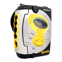
WM-FS473
 Loading...