– 10 –
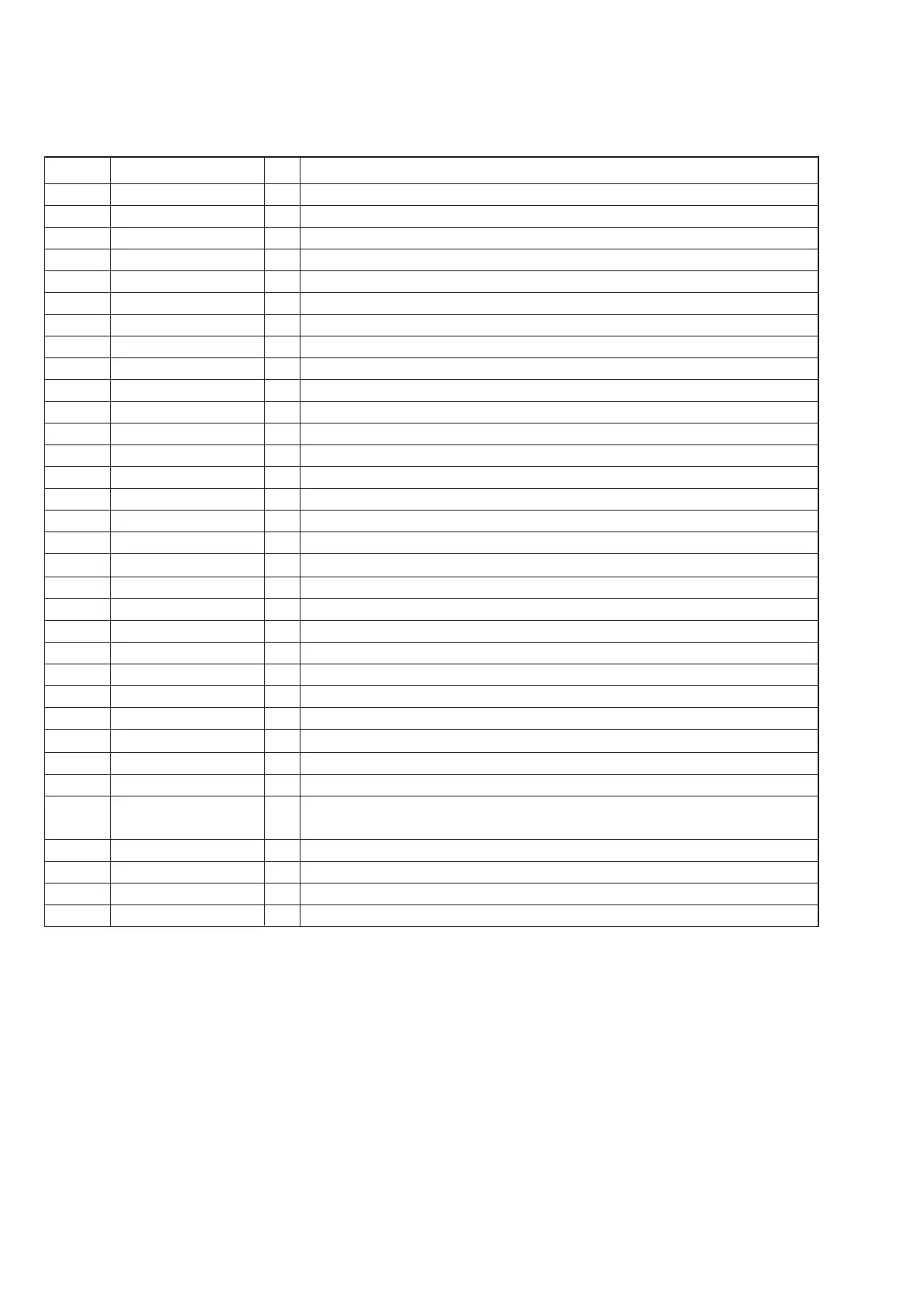
Pin No. Pin name I/O Description
1 – 3 COM1 – COM3 O Common output terminal.
4 – 20 S1 – S17 O Segment output terminal.
21 – 26 KR0 – KR5 O Key return timing output terminal.
27 – 30 K0 – K3 I Key input.
31 – 36 T0 – T5 O Key return timing output.
37 NOM/METAL O Tape normal/metal selection output.
38 TAPE ON I Tape power (MD power) ON Det terminal.
39 LOCAL/DX O Local/DX selection output.
40 MEGA BASS O Mega bass ON/OFF control output.
41 MONO/ST O Mono/Stereo selection output.
42 BAND O FM/AM band selection output.
43 I Power initial terminal.
44 TAPE & RADIO O Tape & Radio +B ON/OFF control.
45 AVLS O AVLS control terminal.
46 BEEP O Beep signal output terminal.
47 MUTE ON O Mute signal output terminal. H : Mute ON
48 TEST I Test terminal (Connected to ground).
–––––––––––––
49 HOLD I Hold detection terminal.
50 IF IN I IF input terminal.
51 RADIO ON O Radio +B ON/OFF control.
52 DO O PLL error signal output.
53 GND – Ground.
54 FM IN I FM local oscillator input terminal.
55 AM IN I AM local oscillator input terminal.
56 VDD – Power supply terminal (+2.8V).
––––––––––––––
57 RESET I System reset terminal. L : Reset
58 X OUT O Crystal oscillator terminal (75kHz).
59 X IN I Crystal oscillator terminal (75kHz).
60 VXT –
Terminal to which external capacitor for stabilization of crystal oscillator power supply is
connected.
61 VLCD – LCD drive power supply set-up terminal.
62 C1 – LCD drive power supply set-up terminal.
63 C2 – LCD drive power supply set-up terminal.
64 VEE – 1.5V constant voltage power supply terminal for LCD drive.
SECTION 5
DIAGRAMS
5-1. EXPLANATION OF IC TERMINALS
IC701 TC9322FB-603 (LCD DRIVE/SYSTEM CONTROL)
 Loading...