10
WM-GX221
SECTION 6
DIAGRAMS
• WAVEFORMS
Note on Schematic Diagram:
• All capacitors are in µF unless otherwise noted. p: pF.
50 WV or less are not indicated except for electrolytics and
tantalums.
• All resistors are in Ω and
1
/
4
W or less unless otherwise specified.
• C : panel designation.
• A : B+ Line.
• H : adjustment for repair.
•Total current is measured with no cassette installed.
•Power voltage is dc 3 V and fed with regulated dc power supply
from external power voltage jack (J401).
•Voltages and waveforms are dc with respect to ground under no-
signal (detuned) conditions.
no mark : FM
(): PB
•Voltages are taken with a VOM (Input impedance 10 MΩ).
Voltage variations may be noted due to normal production toler-
ances.
•Waveforms are taken with a oscilloscope.
Voltage variations may be noted due to normal production toler-
ances.
• Circled numbers refer to waveforms.
• Signal path.
F : FM
f : AM
E : PB
d : REC
N : MIC INPUT
•Abbreviation
5E : E model with the indication of the country of origin.
9E : E model without the indication of the country of origin.
CH : Chinese model
CND : Canadian model
EA : Saudi Arabia model
TW : Taiwan model
Note on Printed Wiring Board:
• Y : parts extracted from the conductor side.
•
a
: Through hole.
Caution:
Pattern face side: Parts on the pattern face side seen from
(Side B) the pattern face are indicated.
Parts face side: Parts on the parts face side seen from
(Side A) the parts face are indicated.
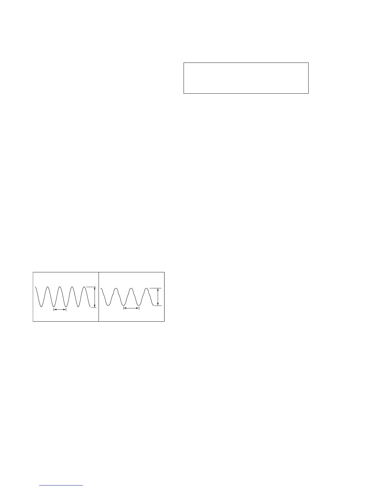
10 V/DIV, 10
µ
s/DIV 1 V/DIV,
2 ms
/DIV
1
T551 (REC mode)
37 Vp-p
22
µ
s
2.5 Vp-p
4.5 ms
2 IC301 r; (VOUT)
(PB mode)
Ver 1.2
 Loading...