
E
Erin JohnsonAug 3, 2025
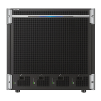
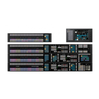
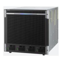
What to do if Sony XVS-8000-C Switch XVS-8000 power does not turn on?
- MMichael BridgesAug 3, 2025
If the Sony Switch XVS-8000 power does not turn on and the AC and DC indicators are not lit green, there are several possible solutions: * Ensure the power switch (A/B/C/D) is turned on. * Verify the power cord is correctly connected. * Press the breaker button.