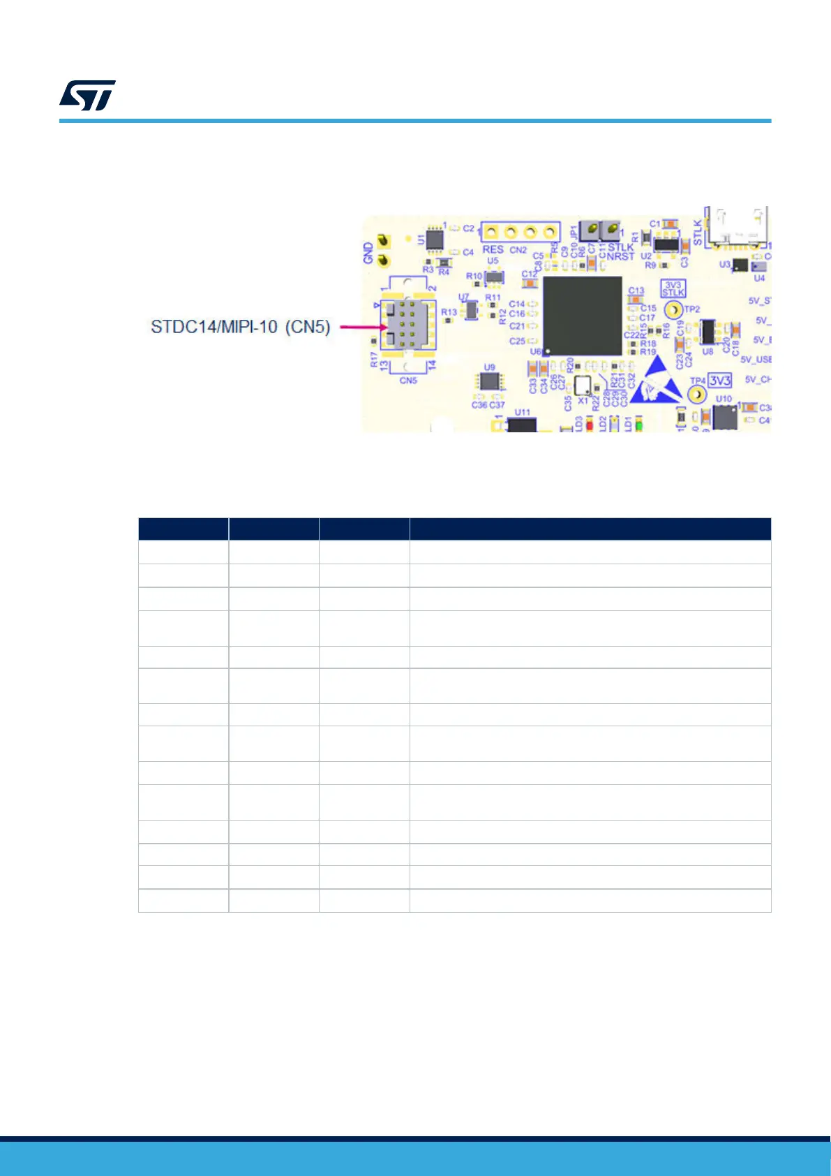
Figure 8 shows the STDC14/MIPI10 connector (CN5).
Figure 8. STDC14/MIPI10 debug connector (CN5)
Table 7
describes the STDC14/MIPI10 connector (CN5) pinout.
Table 7. STDC14/MIPI10 debug connector (CN5) pinout
MIPI10 pin STDC14 pin CN5 Function
- 1 NC
Reserved
(1)
- 2 NC
Reserved
(1)
1 3 VDD
Target VDD
(2)
2 4 T_SWDIO
Target SWDIO using SWD protocol or target JTMS (T_JTMS) using
JTAG protocol
3 5 GND Ground
4 6 T_SWCLK
Target SWCLK using SWD protocol or target JTCK (T_JTCK) using
JTAG protocol
5 7 GND Ground
6 8 T_SWO
Target SWO using SWD protocol or target JTDO (T_JTDO) using JTAG
protocol (SB44 ON)
7 9 NC
T_JRCLK
(3)
/NC
(4)
8 10 T_JTDI
Not used by SWD protocol, target JTDI (T_JTDI) using JTAG protocol,
only for external tools (SB39 OFF)
9 11 GNDDetect
GND detect for plug indicator
(5)
10 12 T_NRST Target NRST
- 13 T_VCP_RX
Target RX used for VCP (with UART supporting bootloader)
(6)
- 14 T_VCP_TX
Target TX used for VCP (with UART supporting bootloader)
(2)
1. Do not connect to the target. It is not connected to the STM32U5 Nucleo-144 board.
2. Input for the external debug tools and output for the STM32U5 Nucleo-144 board.
3. Optional loopback of JTCK on the target side.
4. NC means not required for the SWD connection, not connected on the STM32U5 Nucleo-144 board.
5. Tied to GND. It might be used by the target for the detection of the tool.
6. Output for the external debug tools and input for the STM32U5 Nucleo-144 board.
Two level shifters are used on VCP and SWD interfaces to offer a debug capability with MCU powered by a 1.8 V
power source. The level Shifters are used for signals from target MCU (1.8/3.3 V) to STLINK-V3E (3.3 V).
UM2861
Embedded STLINK-V3E
UM2861 - Rev 5
page 15/49
 Loading...