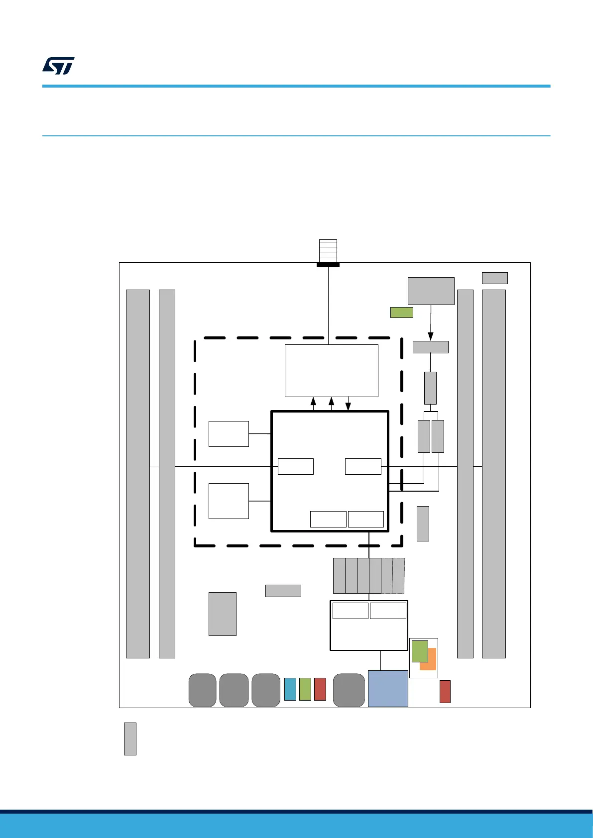
6 Hardware layout and configuration
The STM32WL Nucleo-64 board is designed around the STM32 microcontrollers in a 73-pin UFBGA package.
Figure 3 shows the connections between the STM32 and its peripherals (STLINK-V3E, push-buttons, LEDs, USB,
ARDUINO
®
Uno and ST morpho headers). Figure 4 and Figure 6 show the location of these features on the
STM32WL Nucleo-64 board. The mechanical dimensions of the board are shown in Figure 7.
Figure 3. Hardware block diagram
STM32WL55
Embedded
STLINK-V3E
CN1 USB
Micro-B
connector
B4
RESET
button
ARDUINO
®
ST morpho
GPIO
ARDUINO
®
ST morpho
5V
PWR SEL
DEBUG
BOOT0
LED6
(COM)
32 MHz
Crystal or
TCXO
xxx
LED4 red LED
(OC)
LED1 blue LED (USER)
LED5 green LED
(5V_PWR)
Connectors
or jumpers
B1
USER
button
B2
USER
button
B3
USER
button
LED2 green LED (USER)
LED3 red LED (USER)
RF switch/control
and
RF matching
GND
IDD_RF
GPIO
SMA connector
IDD_SoC
IDD_MCU
5V_PWR
STLK_RST
T_SWDIO
T_SWCLK
T_SWO
STLK_VCP
_TX
T_NRST
STLK_VCP
_RX
VCPSWD
VCPSWD
32 kHz
Crystal
UM2592
Hardware layout and configuration
UM2592 - Rev 1
page 8/49
 Loading...