DocID15687 Rev 5 17/29
PM0059 Flash memory interface
28
unchanged from before the mass-erase operation. The OTP area is not affected by
mass erase and remains unchanged.
Mass erase is performed only when Level 1 is active and Level 0 requested. When the
protection level is increased (0->1, 1->2, 0->2) there is no mass erase.
• Level 2: Disable debug/chip read protection
When the read protection Level 2 is set by writing 0xCC to the RDP option byte:
– All protections provided by Level 1 are active.
– Booting from system memory is not allowed anymore.
– JTAG, SWV (single-wire viewer) are disabled.
– User option bytes can no longer be changed.
– When booting from Flash memory, accesses (read, erase and program) to Flash
memory and backup SRAM from user code are allowed.
Memory read protection Level 2 is an irreversible operation. When Level 2 is activated,
the level of protection cannot be decreased to Level 0 or Level 1.
Note: The JTAG port is permanently disabled when Level 2 is active (acting as a JTAG fuse). As a
consequence, boundary scan cannot be performed. STMicroelectronics is not able to
perform analysis on defective parts on which the Level 2 protection has been set.
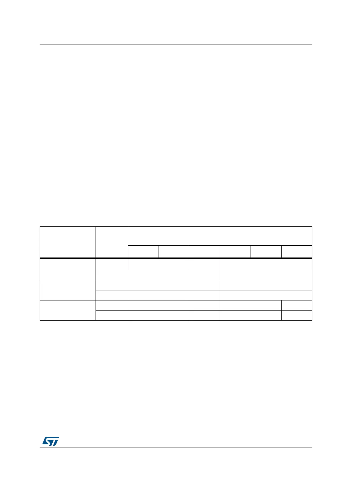
Figure 3 shows how to go from one RDP level to another, and Table 8 summarizes the
memory accesses versus the protection level.
Table 8. Access versus read protection level
Memory area
Protection
Level
Debug features, Boot from RAM or
from System memory bootloader
Booting from Flash memory
Read Write Erase Read Write Erase
Main Flash Memory
and Backup SRAM
Level 1 NO NO
(1)
YES
Level 2 NO YES
Option Bytes
Level 1 YES YES
Level 2 NO NO
OTP
Level 1 NO NA YES NA
Level 2 NO NA YES NA
1. The main Flash memory and backup SRAM are only erased when the RDP changes from level 1 to 0. The OTP area
remains unchanged.
 Loading...


