AN4488 Rev 7 37/50
AN4488 Recommended PCB routing guidelines for STM32F4xxxx devices
49
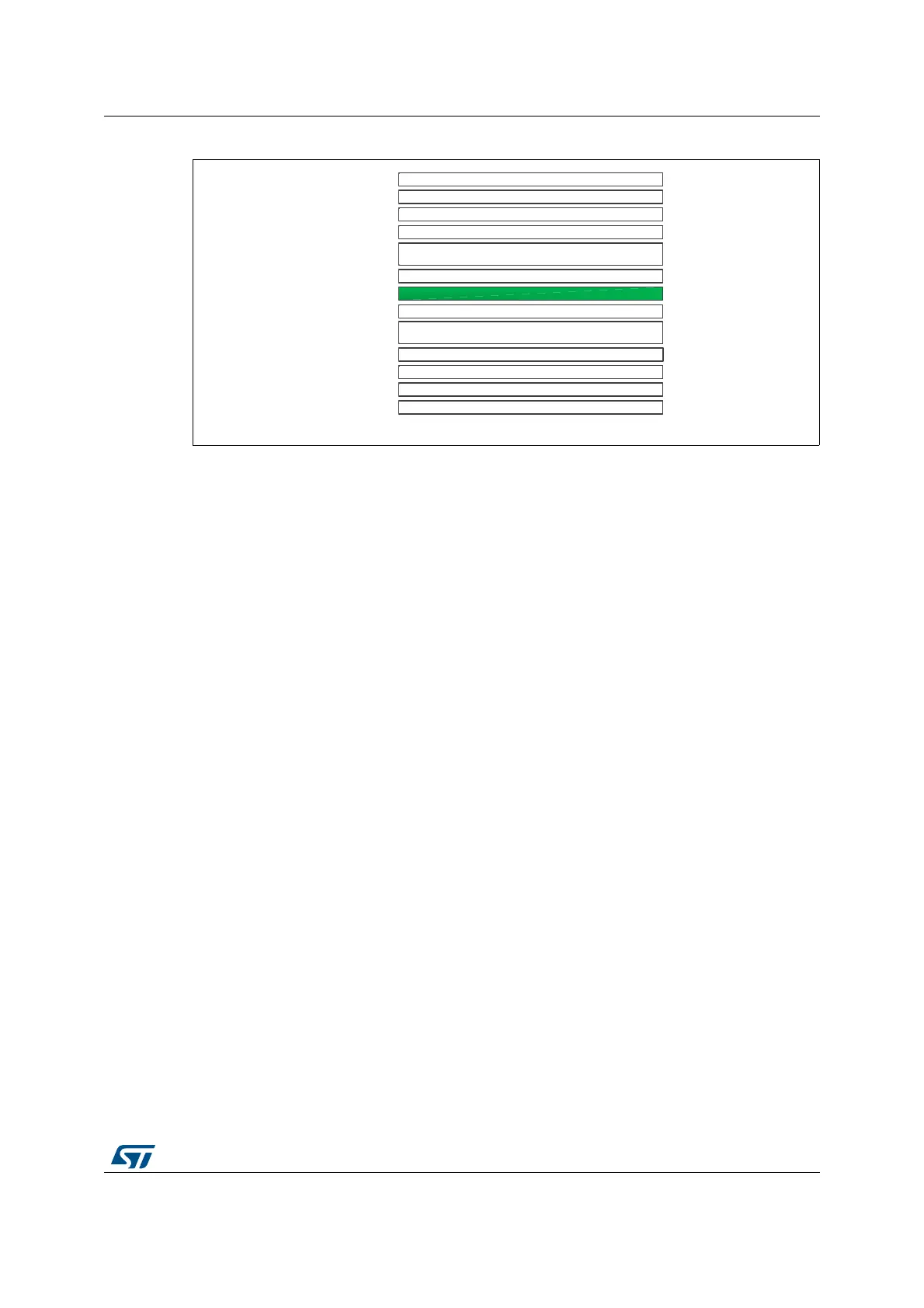
Figure 22. Six layer PCB stack-up example
8.2 Crystal oscillator
Use the application note: Oscillator design guide for STM8S, STM8A and STM32
microcontrollers (AN2867), for further guidance on how to layout and route crystal oscillator
circuits.
8.3 Power supply decoupling
All power supply and ground pins must be properly connected to the power supplies. These
connections, including pads, tracks and vias should have as low impedance as possible.
This is typically achieved with thick track widths and, preferably, the use of dedicated power
supply planes in multilayer PCBs.
In addition, each power supply pair should be decoupled with filtering Ceramic capacitors
(100 nF) and one single Tantalum or Ceramic capacitor (min. 4.7 µF typ.10 µF) connected in
parallel. These capacitors need to be placed as close as possible to, or below, the
appropriate pins on the underside of the PCB. Typical values are 10 nF to 100 nF, but exact
values depend on the application needs. Figure 22 shows the typical layout of such a
VDD/VSS pair.
06Y9
6ROGHU0DVN
+LJK6SHHG6LJQDOV*1'
*1'3ODQH
3RZHU3ODQH
+LJK6SHHG6LJQDOV*1'
3UHSHJ
&RUH
3UHSHJ
6ROGHU0DVN
/D\HUB7RS
/D\HUB,QQHU
/D\HUB,QQHU
/D\HUB%RWWRP
3UHSHJ
/RZ6SHHG6LJQDOV
&RUH
*1'3ODQH
/D\HUB,QQHU
/D\HUB,QQHU
 Loading...


