UM1775 Rev 4 25/39
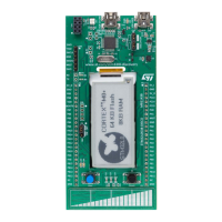
UM1775 Hardware layout
38
6.14 Solder bridges
Table 7. Solder bridges
Bridge State
(1)
Description
SB18, 19 (X2 crystal)
OFF
X2, C47, C50, R70 and R71 provide a clock. PC14, PC15 are disconnected
from P3.
ON PC14, PC15 are connected from P3. Remove only R70 and R71
SB7,8,9,12 (default) ON Reserved, do not modify
SB4,5,6,11 (reserved) OFF Reserved, do not modify
SB14,15 (reserved) OFF Reserved, do not modify
SB29 (B2-RESET)
ON B2 Push Button is connected to NRST of STM32L053C8T6
OFF B2 Push Button is not connected to NRST of STM32L053C8T6
SB22 (B1-USER)
ON B1 Push Button is connected to PA0
OFF B1 Push Button is not connected to PA0
SB2,3 (VCP RX, TX)
(2)
OFF
PA2, PA3 of STM32F103CBT6 are not connected to PA10, PA9 of
STM32L053C8T6
ON
PA2, PA3 of STM32F103CBT6 are connected to PA10, PA9 of
STM32L053C8T6
SB16,17 (USB_USER)
OFF USB1_DP and USB1_DM are dedicated to the USB USER connector CN3
ON
USB1_DP is connected to PA12 and USB1_DM is connected to PA11. Both are
available as GPIO on P2, P3 headers.
SB23,24,25,26,27,28
(touch sensor)
OFF PA2, PA3, PA6, PA7, PB0, PB1 are dedicated to touch sensor.
ON PA2, PA3, PA6, PA7, PB0, PB1 are available as GPIO on P2, P3 headers.
SB1 (ST-LINK/V2-1
PWR)
ON ST-LINK/V2-1 module is powered
OFF ST-LINK/V2-1 module is not powered
SB21 (OSC_IN)
OFF
Clock signal from header P3.7 is connected to OSC_IN of STM32L053C8T6 or
PH0 is available as GPIO. SB20 must be OFF
ON No connection between header P3.7 and PH0 of STM32L053C8T6
SB13 (NRST)
ON
T_NRST signal from connector CN5 and STM32F103CBT6, is connected to
NRST of STM32L053C8T6
OFF T_NRST signal is not connected
SB10 (STM_RST)
OFF No incidence on NRST signal of STM32F103CBT6
ON NRST signal of STM32F103CBT6 is connected to GND
SB20 (MCO)
ON
MCO clock signal from STM32F103CBT6 is connected to OSC_IN of
STM32L053C8T6. SB21 must be OFF
OFF MCO signal of STM32F103CBT6 is not used.
1. Default value is in bold.
2. Default state is OFF for boards labeled MB1143 B-01 and older.