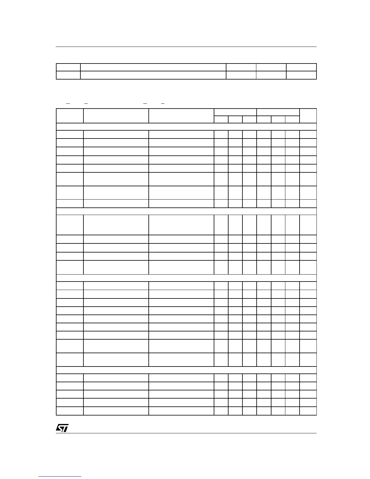
ELECTRICAL CHARACTERISTICS ( [note 1] Unless otherwise stated, these specifications apply for
-25
< T
amb
< 85°C for UC284XB; 0 < T
amb
< 70°C for UC384XB; V
i
= 15V (note 5); R
T
= 10K; C
T
= 3.3nF)
Symbol Parameter Test Conditions
UC284XB UC384XB
Unit
Min. Typ. Max. Min. Typ. Max.
REFERENCE SECTION
V
REF
Output Voltage
T
j
= 25
°
C I
o
= 1mA
4.95 5.00 5.05 4.90 5.00 5.10 V
∆
V
REF
Line Regulation
12V
≤
V
i
≤
25V
220 220mV
∆
V
REF
Load Regulation
1
≤
I
o
≤
20mA
325 325mV
∆
V
REF
/
∆
T
Temperature Stability (Note 2) 0.2 0.2
mV/
°
C
Total Output Variation Line, Load, Temperature 4.9 5.1 4.82 5.18 V
e
N
Output Noise Voltage
10Hz
≤
f
≤
10KHz T
j
= 25
°
C
(note 2)
50 50
µ
V
Long Term Stability
T
amb
= 125
°
C, 1000Hrs
(note 2)
525 525mV
I
SC
Output Short Circuit -30 -100 -180 -30 -100 -180 mA
OSCILLATOR SECTION
f
OSC
Frequency
T
j
= 25
°
C
T
A
= T
low
to T
high
T
J
= 25°C (R
T
= 6.2k, C
T
= 1nF)
49
48
225
52
–
250
55
56
275
49
48
225
52
–
250
55
56
275
KHz
KHz
KHz
∆
f
OSC
/
∆
V
Frequency Change with Volt. V
CC
= 12V to 25V – 0.2 1 – 0.2 1 %
∆
f
OSC
/
∆
T
Frequency Change with Temp. T
A
= T
low
to T
high
–1––0.5–%
V
OSC
Oscillator Voltage Swing (peak to peak) – 1.6 – – 1.6 – V
I
dischg
Discharge Current (V
OSC
=2V) T
J
= 25°C
T
A
= T
low
to T
high
7.8
7.5
8.3
–
8.8
8.8
7.8
7.6
8.3
–
8.8
8.8
mA
mA
ERROR AMP SECTION
V
2
Input Voltage V
PIN1
= 2.5V 2.45 2.50 2.55 2.42 2.50 2.58 V
I
b
Input Bias Current V
FB
= 5V -0.1 -1 -0.1 -2
µ
A
A
VOL
2V
≤
V
o
≤
4V
65 90 65 90 dB
BW Unity Gain Bandwidth T
J
= 25°C 0.7 1 0.7 1 MHz
PSRR Power Supply Rejec. Ratio
12V
≤
V
i
≤
25V
60 70 60 70 dB
I
o
Output Sink Current V
PIN2
= 2.7V V
PIN1
= 1.1V 2 12 2 12 mA
I
o
Output Source Current V
PIN2
= 2.3V V
PIN1
= 5V -0.5 -1 -0.5 -1 mA
V
OUT
High V
PIN2
= 2.3V;
R
L
= 15K
Ω
to Ground
5 6.2 5 6.2 V
V
OUT
Low V
PIN2
= 2.7V;
R
L
= 15K
Ω
to Pin 8
0.8 1.1 0.8 1.1 V
CURRENT SENSE SECTION
G
V
Gain (note 3 & 4) 2.85 3 3.15 2.85 3 3.15 V/V
V
3
Maximum Input Signal V
PIN1
= 5V (note 3) 0.9 1 1.1 0.9 1 1.1 V
SVR Supply Voltage Rejection
12
≤
V
i
≤
25V (note 3)
70 70 dB
I
b
Input Bias Current -2 -10 -2 -10
µ
A
Delay to Output 150 300 150 300 ns
THERMAL DATA
Symbol Description Minidip SO8 Unit
R
th j-amb
Thermal Resistance Junction-ambient. max. 100 150
°
C/W
UC2842B/3B/4B/5B - UC3842B/3B/4B/5B
3/15