Notes :
1. Max package power dissipation limits must be respected; low duty cycle pulse techniques are used during test maintain T
j
as
close to T
amb
as possible.
2. These parameters, although guaranteed, are not 100% tested in production.
3. Parameter measured at trip point of latch with V
PIN2
= 0.
4. Gain defined as :
∆
V
PIN1
A = ; 0
≤
V
PIN3
≤
0.8 V
∆
V
PIN3
5. Adjust V
i
above the start threshold before setting at 15 V.
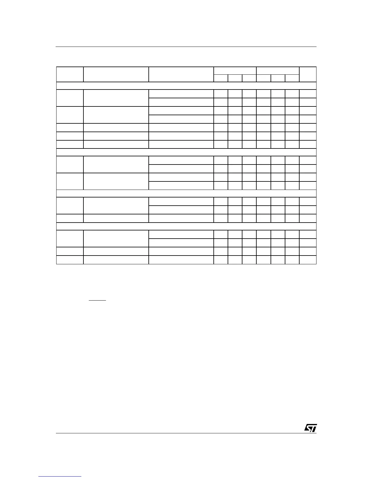
ELECTRICAL CHARACTERISTICS (continued)
Symbol Parameter Test Conditions
UC284XB UC384XB
Unit
Min. Typ. Max. Min. Typ. Max.
OUTPUT SECTION
V
OL
Output Low Level I
SINK
= 20mA 0.1 0.4 0.1 0.4 V
I
SINK
= 200mA 1.6 2.2 1.6 2.2 V
V
OH
Output High Level I
SOURCE
= 20mA 13 13.5 13 13.5 V
I
SOURCE
= 200mA 12 13.5 12 13.5 V
V
OLS
UVLO Saturation VCC = 6V; I
SINK
= 1mA 0.1 1.1 0.1 1.1 V
t
r
Rise Time
T
j
= 25
°
C C
L
= 1nF (2)
50 150 50 150 ns
t
f
Fall Time
T
j
= 25
°
C C
L
= 1nF (2)
50 150 50 150 ns
UNDER-VOLTAGE LOCKOUT SECTION
Start Threshold X842B/4B 15 16 17 14.5 16 17.5 V
X843B/5B 7.8 8.4 9.0 7.8 8.4 9.0 V
Min Operating Voltage
After Turn-on
X842B/4B 9 10 11 8.5 10 11.5 V
X843B/5B 7.0 7.6 8.2 7.0 7.6 8.2 V
PWM SECTION
Maximum Duty Cycle X842B/3B 94 96 100 94 96 100 %
X844B/5B 474850474850 %
Minimum Duty Cycle 0 0 %
TOTAL STANDBY CURRENT
I
st
Start-up Current V
i
= 6.5V for UCX843B/45B 0.3 0.5 0.3 0.5 mA
V
i
= 14V for UCX842B/44B 0.3 0.5 0.3 0.5 mA
I
i
Operating Supply Current V
PIN2
= V
PIN3
= 0V 12 17 12 17 mA
V
iz
Zener Voltage I
i
= 25mA 30 36 30 36 V
UC2842B/3B/4B/5B - UC3842B/3B/4B/5B
4/15