10
LX-100
I/O CIRCUIT AND WIRING DIAGRAMS
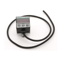
SPOT SIZE CHARACTERISTICS (TYPICAL)
NPN output type
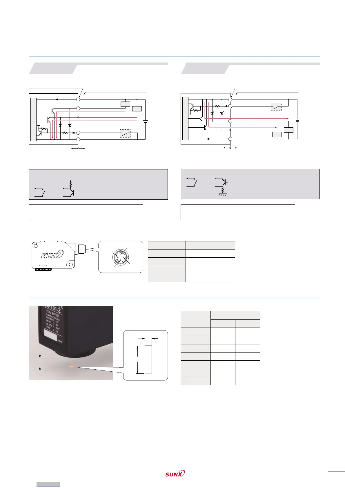
I/O circuit diagrams
Users’ circuitInternal circuit
D1
D2
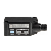
Color code of cable type /
mating cable for plug-in connector type
(Brown)
V
(Black) Output 1
50 mA max.
50 mA max. (Note 1)
(White) Output 2 (Note 2)
ZD1
ZD2
(Blue) 0 V
Tr1
Tr2
10 kΩ
D2
10 kΩ
(Pink) Teaching input
m1
5 V
Load
Load
3
1
Terminal No. of plug-in connector type
12 to 24 V DC
10 %
Notes: 1)
The current of the plug-in connector type LX-101-Z is 100 mA max.
2)
The output 2 is not incorporated to the plug-in connector type LX-101-Z.
Notes: 1)
The current of the plug-in connector type LX-101-Z is 100 mA max.
2)
The output 2 is not incorporated to the plug-in connector type LX-101-Z.
m1
Non-voltage contact or NPN transistor
or
High:
5 V to V, or open
Low:
0 V to 2 V (source current: 0.5 mA or less)
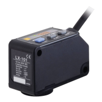
Users’ circuitInternal circuit
Sensor circuit
PNP output type
ZD1
ZD2
(Brown) V
(Pink) Teaching input
D1
Tr1
Tr2
50 mA max. (Note 1)
50 mA max.
(Black) Output 1
(Blue) 0 V
(White) Output 2
(Note 2)
0 V
m1
Color code of cable type /
mating cable for plug-in connector type
12 to 24 V DC
10 %
4
1
Load
Load
Terminal No. of plug-in connector type
m1
Non-voltage contact or PNP transistor
or
High: 4 V to V (sink current: 3 mA or less)
Low: 0 V to
0.6 V, or open
I/O circuit diagrams
3
Layout of connector pin of plug-in connector type
(Unit: mm in)
2 0.079
1.7 0.067
1.2 0.047
1.0 0.039
1.3 0.051
1.5 0.059
2.0 0.079
7 0.276
8 0.315
9 0.354
10 0.394
11 0.433
12 0.472
13 0.512
Setting distance L
(Note 1)
Width (W)
Spot size (Note 2)
V
Teaching input
0 V
Output
1
2
3
4
Connector pin No.
Description
5.5 0.217
5.5 0.217
5.3 0.209
5.0 0.197
5.0 0.197
5.0 0.197
5.0 0.197
Length (D)
3
4
2
1
V
0 V
L
D
W
4
2
2
Sensor circuit
Symbols... D1, D2 : Reverse supply polarity protection diode
Z
D1, ZD2: Surge absorption zener diode
T
r1, Tr2 : NPN output transistor
Symbols... D1, D2 : Reverse supply polarity protection diode
Z
D1, ZD2: Surge absorption zener diode
T
r1, Tr2 : PNP output transistor
Notes: 1)
2)
Setting distance ‘L’ represents the
distance from the lens surface to
the sensing object.
Examples only meant for use as a
guideline.