14
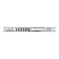
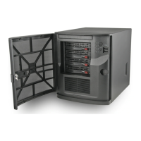
SuperServer 5019A-12TN4 User's Manual
Figure 1-5. System Chipset Block Diagram
Note: This is a general block diagram and may not exactly represent the features on your
motherboard. See the System Specications appendix for the actual specications of your
motherboard.
Connector Description
JTGLED1 LAN5/LAN6 Acitivity LED Header
JTPM1 Trusted Platform Module/Port 80 Connector
LAN1 ~ LAN4 LAN1 - LAN4: GbE LAN (RJ45) Ports
SLOT7 CPU PCI-E 3.0 x4 Slot
SRW1, SRW3, SRW4 M.2 Holding Screws
UID Unit ID Button
USB0/1 Back panel Universal Serial Bus (USB) 3.0 Ports
USB2/3, USB4/5 Front Accessible USB 2.0 Headers
VGA VGA Port
8.5mm
2133MHz
DDR4 (CHA)
DIMMA1,A2
DDR4 (CHB)
DIMMB1,B2
2133MHz
AST2400
COM1 HEADER
TPM1.2 Header
LPCHSIO[10]
PCIEX1
LAN PORT1
LAN PORT2
SVID
VR13
VGA
SATA/PCIE SSD
M.2 2280/2242
PCIe 3.0_x4
8GT/s
PCIE SLOT X4
PCIe 3.0_x4
8GT/s
HSIO[3:0]
PCIE x4
HSIO[7:4]
PCIE x4
HSIO[9:8]
i350 Lan x4
SATA-III
6Gb/s
HSIO[17:14]
RJ45
RTL8211F
RGMII2
GIGALAN
SGPIO[0]
4 X SATA-III
USB 3.0 Rear IO
5Gbps
USB3.0
HSIO[19:18]
USB3.0
GL854G
USB2.0[1]
4 X USB 2.0
( Header x2 )
480Mbps
USB2.0
USB2.0[3:2]
USB2.0[0]
Intel
FCBGA1310
PCIe 3.0_x2
8GT/s
Mini PCIE/mSATA
PCIe 3.0_x1
8GT/s
HSIO[12]
 Loading...