3-22
X8DTN+-F/X8DTN+-F-LR User's Manual
Power Button
OH/Fan Fail LED
1
NIC1 LED
Reset Button
2
Power Fail LED
HDD LED
Power LED
Reset
PWR
Vcc
Vcc
Vcc
Vcc
Ground
Ground
1920
Vcc
X
Ground
NMI
X
Vcc
NIC2 LED
Power LED
The Power LED connection is located
on pins 15 and 16 of JF1. Refer to the
table on the right for pin defi nitions.
NMI Button
The non-maskable interrupt button
header is located on pins 19 and 20
of JF1. Refer to the table on the right
for pin defi nitions.
NMI Button
Pin Defi nitions (JF1)
Pin# Defi nition
19 Control
20 Ground
Power LED
Pin Defi nitions (JF1)
Pin# Defi nition
15 +5V
16 Ground
Front Control Panel Pin Defi nitions
A. NMI
B. PWR LED
A
B
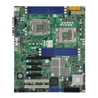
JBAT1
LE2
JPI2C1
JD1
JPP0
JPP1
JP7
JP5
JWOR1
JI2C1
JI2C2
LE1
LEM1
FAN4
FAN3
FAN2
FAN7
FAN5
FAN6
SP1
JF1
JWD
JPL1
JPB
JPW2
JPW3
JTPM1
SW1
JWF1
JPW1
USB4/5
USB6/7
USB10
UID
IPMI_LAN
USB2/3
ALWAYS POPULATE DIMMxA FIRST
P1 DIMM3B
P1 DIMM3A
P1 DIMM2C
P1 DIMM2B
P1 DIMM2A
P1 DIMM3C
P1 DIMM1C
P1 DIMM1B
P1 DIMM1A
P2 DIMM3A
P2 DIMM3B
P2 DIMM3C
P2 DIMM2A
P2 DIMM2B
P2 DIMM2C
P2 DIMM1A
P2 DIMM1B
FAN8/CPU1
CPU2
I-SATA5
I-SATA4
I-SATA3
I-SATA2
I-SATA1
USB8
Slot6 PCI-E 2.0 x8 (In x16 Slot)
Slot5 PCI-E x4 (In x8 Slot)
Slot4 PCI-E 2.0 x8 (In x16 Slot)
Slot3 PCI-E 2.0 x4 (In x8 Slot)
Slot2 PCI-E 2.0 x4 (In x8 Slot)
LAN2
VGA (Bottom)
COM1 (Top)
KB/MOUSE
P2 DIMM1C
I-SATA0
PWR I2C
FAN7/CPU2
CPU1
USB0/1
T-SGPIO2
LAN1
Slot0 PCI-U
COM2
PHY
IPMB
JL1
T-SGPIO1
Intel ICH10R
South Bridge
BIOS
Intel IOH36
FP CTRL
JPG1
ALWAYS POPULATE DIMMxA FIRST
X8DTN+-F
Rev. 2.00
LAN CTRL
BMC CTRL
FAN1
JBT1
 Loading...