SP1
+
+
B1
JBT1
IPMB
JD1
JPW1
JPW2
JPI2C
JWOL
JWF1
JF1
FAN2
FAN1
FAN5
FAN3
FAN4
T-SGPIO1 T-SGPIO2
JI2C1
JI2C2
JWOR
JL1
3
JPUSB1
JLED
JPL1
JPL2
JPG1
LE1
C
C
LE7
J*
W83627DHG
IDT
89HI0524G2PS
PCH
Hermon
SLOT7 PCI-E 2.0 (2.5GT/s) X1
SLOT6 PCI-E 2.0
SLOT5 PCI-E 2.0 X8
SLOT4 PCI-E 2.0 X8
SLOT3 PCI-E 2.0 (2.5GT/s) X1
USB8/9
FAN2/CPUFAN
USB4
USB5
FAIL
PWR
DOM PWR
JWOL:
I-SATA4
I-SATA3
UID
DIMM2A
DIMM2BDIMM2CDIMM1B DIMM1A
Chassis Intrusion
Wake on Lan
Wake on Ring
CMOS CLEAR
1-2:ENABLE
2-3:DISABLE
JPL2:LAN2
JPL1:LAN1
2-3:DISABLE
1-2:ENABLE
JPB:BMC
JPI2C:PWR I2C
JSPK:Buzzer/Speaker
COM2
FLOPPY
DDR3 1066/1333 UDIMM/RDIMM required
JL1:
LAN1/LAN2
JPUSB1:B/P USB WAKE UP
1-2:ENABLE
2-3:DISABLE
JI2C1/JI2C2
USB6/7
2-3:Disable
1-2:Enable
CPU
JLED:Power LED
OFF:Disable
ON:Enable
2-3:DISABLE
1-2:ENABLE
JF1
ON
LED LED
PWRHDD
NIC1
NIC2
OH/FF
RST
PWR
I-SATA2
I-SATA1
I-SATA0
I-SATA5
SLOT2 PCI-E 2.0 (2.5GT/s) X4 (IN X8 SLOT )
SLOT1 PCI 33MHz
DIMM1C
JPG1: VGA
KB/MOUSE
VGA
COM1
IPMI_LAN
USB0/1
USB2/3
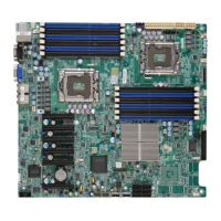
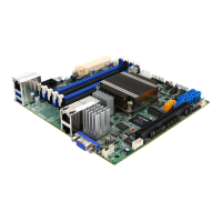
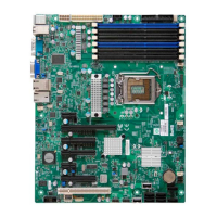
X8SIA
Serial_Link-SGPIO
PinDenitions
Pin# Denition Pin Denition
1 NC 2 NC
3 Ground 4 DATA Out
5 Load 6 Ground
7 Clock 8 NC
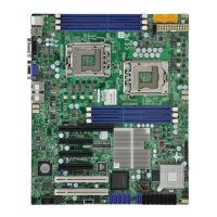
T-SGPIO 0/1 Headers
Two T-SGPIO (Serial-Link General Pur-
pose Input/Output) headers are located
near the SATA connectors on the moth-
erboard. These headers are used to
communicate with the enclosure manage-
ment chip in the system. See the table on
the right for pin denitions. Refer to the
board layout below for the locations of
the headers.
NC: No Connections
A. T-SGPIO 1
B. T-SGPIO 2
C. SATA DOM Power
C
A
B
SATA DOM Power
The SATA DOM Power on JWF1 is used
to supply power to SATA Disk-On-Module
(DOM) solid-state storage devices.
 Loading...