t
;
I
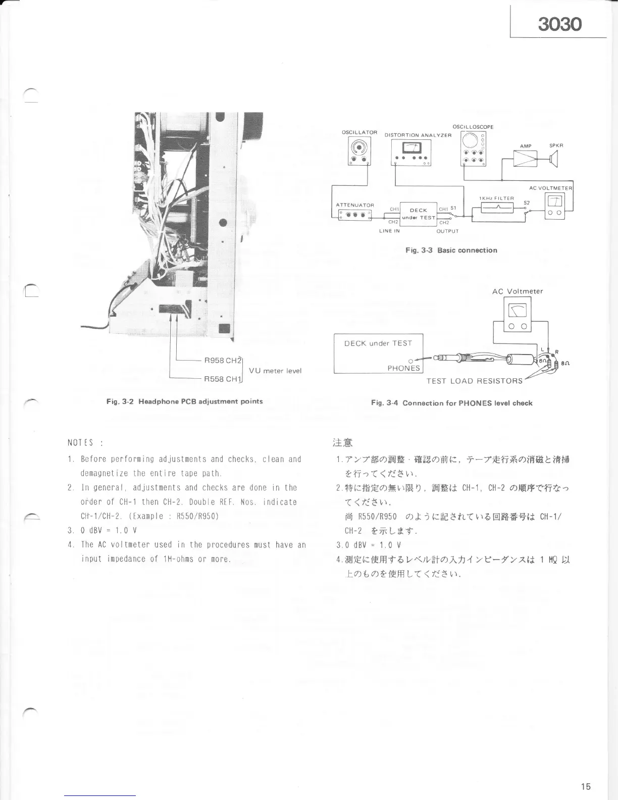
Fig.3-2 Headphone PCB adjustment
points
NOI tS
:
1. Before
perf0rtning
adlustments and checks, clean and
delnagnet ize the enti fe
tape
path.
2.
In
general,
adjustntents and checks
are done in the
0fder 0f Ci]-1 then CH-2. Double RIF.
Nos, indicate
Cll-l/C|.l-2.
(txample
: R550/R950)
3.0dBV=1.0V
4. The AC v0l tI|leter used in
the
procedures
|tlust have
an
i nput impedance
of 1H-ohms
0r
lll0re.
LINE IN
Fig.
3-4
Connection
for
PHONES
level check
it,a
1.7
>7ffioffi&
.
MZLoffiIx, i-7ft.',fr*/)iHBL
iHtfi
t'fi',(
(
/jE lt.
2.++titFft.a*!\[E
D, AfilBlJ
CH-1, cT-z
a]EftT'frfc ")
( (
/i3
t,t.
r{
Rs50/R950
/)}
i {t;d,3fL(lr5gg*utJ
cH-1/
cl|-2
tzrL*,f.
3.0 dBv
=
1.0
v
4.WlEirlHHf
bv<)va+a^fi4
Yv-yvxtJ
1 HQ
ttl
La{rattf.ffi L(
(
t3
t,r.
oscr
LLoscoPE
DECK
under
TEST
AC Voltmeter
TEST
LOAD RESISTORS
15


 To Next Page