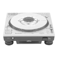
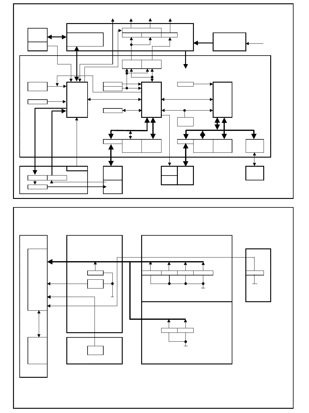
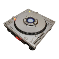
DZ1200 system block diagram
Fig 1 H.PHONE DIGITAL Refer to the item "Com
osition of the
arts".
LINK LINE OUT OUT OUT Refer to the item "Outline of the
arts".
JACK
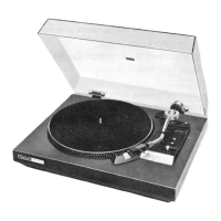
Turntable AMP AMP BUFFER POWER
VCC
Sensor AC100V~240V
MAIN
DAC DIGITAL
PCM1734 TC9271
VCC
4.5 V monitoring
27MHz 27MHz
RESET
Microcomputer
11.29MHz DSC25 DSC25
(SC microcomputer)
(MD microcomputer)
M30622 Serial Serial
16MHz
(UI microcomputer)
I2C
EEROM
ADC IN
2.9 V monitoring
RESET
External bus External bus
Buffer FLASH SDRAM Buffer FLASH SDRAM SD I/F
ROM X2 ROM MN5772
CP TEMPO VR Shutter
LCD CD SD
Decoder LED
SW
LED LED
DZ1200 SW, VOLUME input circuit block diagram
Refer to the item "Signal flow", panel.
Fig 2
MAIN CP1 CP3
IC2 CP2
UI microcomputer
A/D
M30622 input SW10~40
SW x6 SW x9 SW x8 SW x3 SW x4 REV SW
A/D
input CD/SD CD/SD
SW DE
A/D DE
input PCON
A/D DE
input REV CP5
SW x5 SW x4
IC14 P-CON
Scratch microcomputer
DSC25 TEMPO DE
VR
Refer to the item "Explanation of the main signals".
MUTE
Motor
Controller AN6680
Driver AN6675
Switching power supply
ATAPI interface
SW
Serial
communication