A
B
c
o
E
F
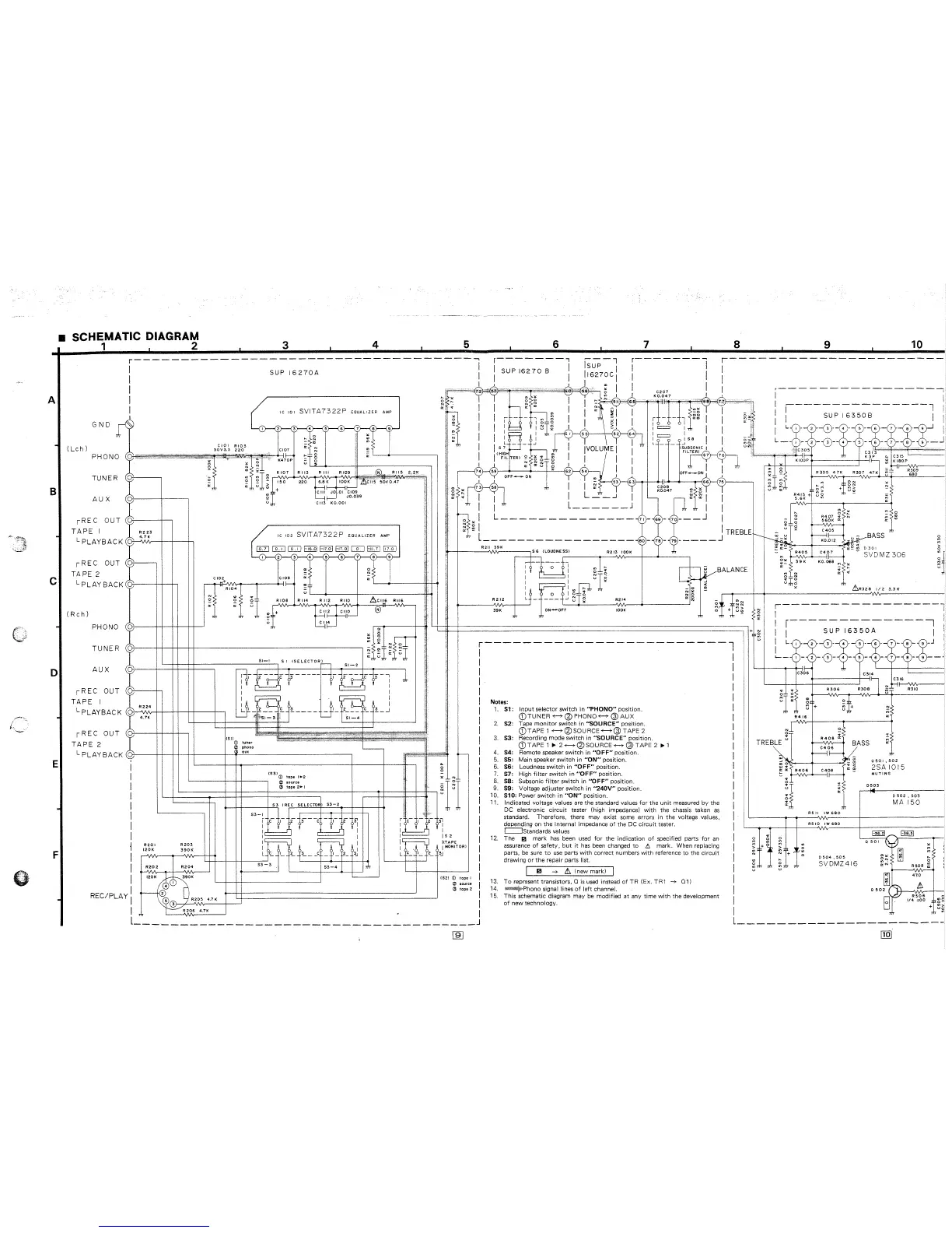
• SCHEMATIC DIAGRAM
1 2
3
4 5
6
7
8
9
10
r-----------------------------------~
1
SUP
16270A
:
r-------,
---l
r--------
I
SUPI6270B
I
Isup
I I I
r----------------------
I
I I
I
,"':'c
cc"'--_---4
c
7c2
1 I
116270C
1
I 1
•
57:1-'c.
;;:;';;~:":':"";~;';"':':"':':":':';';";;:;';;-'{~
c~
I I
C207
I,
I
I
1
~~~
m !le Y
Y'
~
KO.047
~ ~
I 1
~
~'"
y
.~
,",,":;""".-:-.,.--"""{MI
1---
-
-------------:
I
I
---------------l
i
1
1 C
10
I
GND
(Lch)
SVITA7322P
o
...
N
=
co
'"
N
N
6
EQUALIZER
AMP
8 9
PHONO
"'n=~
: I
'"
L-_.
______
~
TUNER
AUX
r
REC
OUT
((
cri}'---t--
TAPE I
LpLAYBACK
r
REC
OUT
R223
4.7K
- 0
U
~
RI13
Rill
RI09
,®
'0",~115
220
~C8j~100K~C'iI5
50VO.47
CIII
JO.Oli~
JO.039
CII3
KO.OOI
~
c
102
SVITA7322P
EQUALIZER
AMP
lID
[£J]
C£:::D
1-16.011-17.011-17.01
CIJ
EiQJ
GI:Q]
123456789
o
N
;;<
TAPE
2
LpLAYBACK(,~--~~
L-
__
+-
______
~~~
(Rc
h)
N
o
'"
RI08
~,
+
R 114
R 112
RIIO
@
PHONO(
(,~----++-++-~~
U
GI~O
~I~
~
~l
Nr:r
TU
NE
R
\..u07---+-+-++-~-----------------_.,
- : l
N?~-L
51-1
SI
ISELECTOR)
~m~I"'rIr
~I
AUX
rREC
OUT
TAPE
I
L
PLAYBAC
K
rREC
OUT
TAPE 2
L
PLAYBACK
I
I
I
I
I
I
I
I
j
1
R224
4.7K
R201
120K
L-~+--++-_____________________
~
S{-2
8'~ci3------i'~~-~3-1
I I
I
L~)
.
r-'
I
I
UI
-J~~£.
h
____
J _
~I_
2~~
C_
~_J
Lt
4l1?-s1-3.
-T
Lf
51-4
~--4--~----~---*~
L---+--r------~
(511
CD
tuner
l2l
phono
~
cux
-
(S3)(J)
tope
'.2
'-------+-+-1---,
!2>
source
R203
390K
53-3
G
tape
2.'
53-4
!
..
o
o
3
l
I
I
N
"'.",
f----;"'h:
I I
~il-
~I
I
I'
- \ -
~I
~-L~
I I
~
~~..J!
I,
r - -
I '-'=::! I
~Ig
I j : =
up-
J,.
'1
1
'
'I~OLU~J11
!
0==_
?;g
I
.,
"'co
I
:m
I
J
58
I
{SUBSONIC,
I
F1L~
- ;
0"
"'-
'"
'
i
l:~_
2
~-~~~.~3
:o~
"-Q-qJ-J
i
L_
1-
2
-0--¥-
5 -
6)--ct>--<$--d)--J
C~~5
C313
.
'L-----1r-..,--+-!1
r-'
K 3 P .. C
315
I
FILTER)
~
~5
~-L~
I I I
N
C\I
N 0
~
II
",couo~I'
I
74
59
'"
62
54
_
I,
I
OFF-ON
""'Hi'
co
~
1 I
~
53
6
3hrl---<C>-i20f-8----.....,6~
l Y
7;6
l
OFF_ON!
!
75)----
1
KIOOP
:l
to
KI80P
'"
'"
b-1
~l
~
R305
47K
R307
47K
~
~
~I~m
~2
+±~~
~?
~
51!
! 1 I L m _ -J I KO.047
~ ~
1
I I L
______
j
Ttr
I
~
'"
I L
______________
71
-
69-
70---
J
~
~
I
1
~:~~
+ U
~
ro'l
1 I
...
I
c;lg
R407
560K
'"
~
0
'"
'"
It
'"
T L
________________
_
80
-
78-
J
1
TREBLEr----
UJ
~
g
~f'-=-
_ BASS m
79
-----
r---M?
KO,Ol2
~~
R211
39K
~-+------'IN\r------'
5 6
(LOUDNESSI
R213
lOOK
~:~
a::~~
D301
-
'"
.....,Rv4\/'0v-5-+-_C4-1r~
-
SVDMZ
306
R
212
39K
lOOK
1
+ N
!
,
i
r------------------------l
I I
I I
I 1
I I
I I
I
Notes: I
I
1.
Sl:
Input
selector
switch
in
"PHONO"
position.
1
CD
TUNER
+-?- @
PHONO
+-?- @
AUX
I
2.
S2:
Tape
monitor
switch
in
"SOURCE"
position. I
I
CDTAPE
1 -<---+@SOURCE-<---+@
TAPE
2
3.
S3:
Recording
mode
switch
in
"SOURCE"
position.
I
f~
u
(j)TAPE
1
~
2-<---+@SOURCE+-?-@TAPE
2
~
1 I
4.
S4:
Remote speaker
switch
in
"OFF"
position.
I
5.
SS: Main speaker
switch
in
"ON"
position.
6.
S6:
Loudness
switch
in
"OFF"
position. I
7.
S7:
High
filter
switch
in
"OFF"
position.
I
8.
S8:
Subsonic
filter
switch
in
"OFF"
position.
I
9. S9: Voltage adjuster
switch
in
"240V"
position.
1
O.
S10:
Power
switch
in
"ON"
position.
I
11. Indicated voltage values are
the
standard values
for
the
unit
measured
by
the
I
DC
electronic
circuit
tester (high impedance)
with
the
chassis taken
as
1
standard.
Therefore,
there may exist some errors in
the
voltage values,
depending on
the
internal
impedance
of
the DC
circuit
tester. I
c:::=JStandards
values
O~
39K
KO
068
~-
.
"'50'"
'"
N
o N
"TO
Urtro
x
RS
11
"
...
'"
"
!
"
'"
IW
680
m
Ir
RSIO
IW
680
L!:.R328
1/2
3.3K
N
'"
'"
rfr
MUTING
0503
0502,503
MA
150
IS
2
I(TAPE
12.
The
I1J
mark
has
been used
for
the
indication
of
specified parts
for
an
assurance
of
safety,
but
it
has
been changed
to
L!l
mark.
When replacing
parts,
be
sure
to
use
parts
with
correct numbers
with
reference
to
the
circuit
drawing
or
the
repair
parts list.
I
I MONITOR}
~
(52)
CD
tape
I
(2)
louree
13
tape
2
I
I1J
-r
L!:. (new mark) I
To
represent transistors, 0
is
used instead
of
TR
(Ex. TR1
-r
01)
~'Phono
signal lines
of
left
channel.
U)
o
",
u
T
...
o
'"
u
7
0504,505
SVDMZ416
x
'"
'"
...
o
R50e
~
410
AY
i
~~::::
~::::
REC/PL
I 5 3
R205
4.7
K I
l
R206
4.7K
• 1
13.
14.
15.
This
schematic diagram may
be
modified
at
any
time
with
the
development
of
new
technology.
I
I
I
1
1
I
I
RSO
6
114 :100
C
"'c
0-
+
"'>
Uc
'"
---
_________________________________
J
l
___________________
--
am