Do you have a question about the Technics SU-VX920 and is the answer not in the manual?
Detailed power and distortion specs for the main amplifier.
Input sensitivity and impedance for preamp stage.
Power consumption, dimensions, weight, and other general specs.
Precautions and initial steps before performing repairs or adjustments.
Explains the amplifier's protection features and troubleshooting.
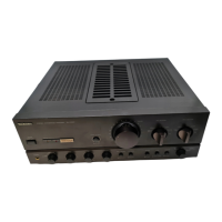
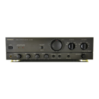
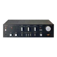
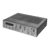
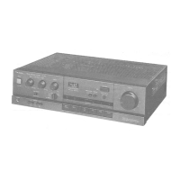
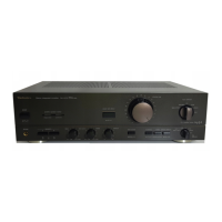
The main power button and status lights.
Adjustments for sound level and channel balance.
Adjustments for bass and treble frequencies.
Controls for choosing audio sources and recording destinations.
Controls for speaker output and phono cartridge type.
Switches for Loudness, Muting, Mode, and Adaptor functions.
Port for connecting headphones.
Connects to a CD player's line output.
Connects to a tuner's line output.
Connects to a turntable's audio output.
Connects to a tape deck or DAT player's I/O.
Connects to auxiliary audio sources like video players.
Connects to a primary tape deck's audio I/O.
Direct input to the power amplifier section.
For connecting external audio processing devices.
Steps for removing outer panels and chassis components.
Procedures for removing power transformer and capacitor block.
Steps to detach front panel, switches, and volume controls.
Procedures for removing various internal PCBs.
Steps to detach the rear panel and power transistors.
Schematic of the input selection circuitry.
Schematic of the tape/DAT input/output circuit.
Schematic of the main operational control circuits.
Schematic of the audio volume control circuit.
Schematic for AC power input and voltage adjustment.
Schematic of the capacitor block circuitry.
Schematic of the headphone output circuit.
Diagram of the main printed circuit board layout.
Diagram of the operation control printed circuit board.
Diagram of the tape/DAT input/output printed circuit board.
Diagram of the volume control printed circuit board.
Diagram of the AC inlet and voltage adjustment board.
Diagram of the input selector printed circuit board.
Diagram of the capacitor block printed circuit board.
Diagram of the power switch/headphone jack PCB.
| Total Harmonic Distortion (THD) | 0.02% (20Hz-20kHz, 8Ω) |
|---|---|
| Frequency Response | 5 Hz - 100 kHz |
| Damping Factor | 100 |
| Input Sensitivity | 150mV (line) |
| Speaker load impedance | 4 ohms to 16 ohms |
| Dimensions | 430 x 125 x 344mm |