Theory of Operation—2213 Service
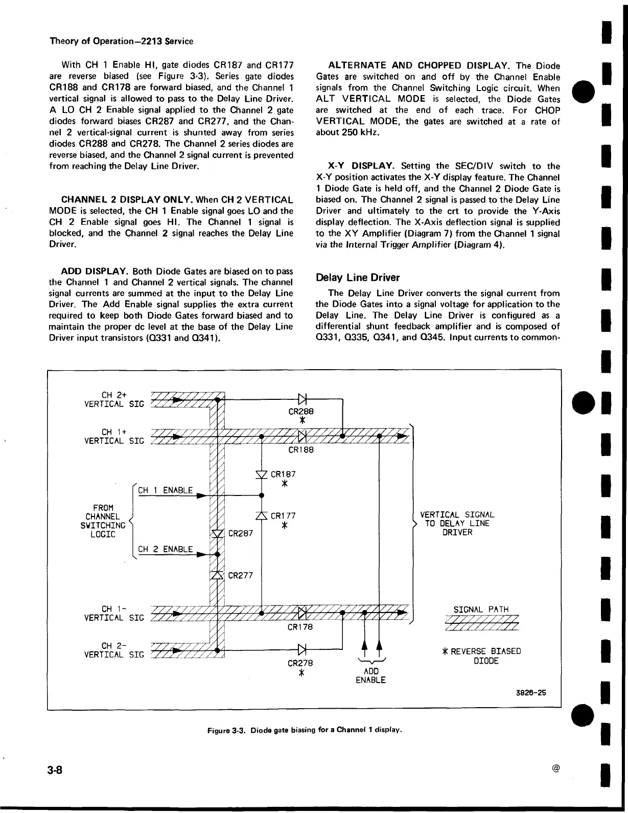
With CH 1 Enable HI, gate diodes CR187 and CR177
are reverse biased (see Figure 3-3). Series gate diodes
CR188 and CR178 are forward biased, and the Channel 1
vertical signal is allowed to pass to the Delay Line Driver.
A LO CH 2 Enable signal applied to the Channel 2 gate
diodes forward biases CR287 and CR277, and the Chan
nel 2 vertical-signal current is shunted away from series
diodes CR288 and CR278. The Channel 2 series diodes are
reverse biased, and the Channel 2 signal current is prevented
from reaching the Delay Line Driver.
CHANNEL 2 DISPLAY ONLY. When CH 2 VERTICAL
MODE is selected, the CH 1 Enable signal goes LO and the
CH 2 Enable signal goes HI. The Channel 1 signal is
blocked, and the Channel 2 signal reaches the Delay Line
Driver.
ADD DISPLAY. Both Diode Gates are biased on to pass
the Channel 1 and Channel 2 vertical signals. The channel
signal currents are summed at the input to the Delay Line
Driver. The Add Enable signal supplies the extra current
required to keep both Diode Gates forward biased and to
maintain the proper dc level at the base of the Delay Line
Driver input transistors (Q331 and Q341).
ALTERNATE AND CHOPPED DISPLAY. The Diode
Gates are switched on and off by the Channel Enable
signals from the Channel Switching Logic circuit. When
ALT VERTICAL MODE is selected, the Diode Gates
are switched at the end of each trace. For CHOP
VERTICAL MODE, the gates are switched at a rate of
about 250 kHz.
X-Y DISPLAY. Setting the SEC/DIV switch to the
X-Y position activates the X-Y display feature. The Channel
1 Diode Gate is held off, and the Channel 2 Diode Gate is
biased on. The Channel 2 signal is passed to the Delay Line
Driver and ultimately to the crt to provide the Y-Axis
display deflection. The X-Axis deflection signal is supplied
to the XY Amplifier (Diagram 7) from the Channel 1 signal
via the Internal Trigger Amplifier (Diagram 4).
Delay Line Driver
The Delay Line Driver converts the signal current from
the Diode Gates into a signal voltage for application to the
Delay Line. The Delay Line Driver is configured as a
differential shunt feedback amplifier and is composed of
Q331, Q335, Q341, and Q345. Input currents to common-
ENABLE
3826-25
3-8
Figure 3-3. Diode gate biasing for a Channel 1 display.
 Loading...


