Theory of Operation
3–8
TDS 340A, TDS 360 & TDS 380 Technical Reference
-!! *
%(
%($ *
#% +
'&,*'$$ *
)-#+#,#'&
%'*0
*#"" *
'"#
&$'"
*#"" *
%($#!# *
%($#!# *
(,#'&
'*+
-+
/, *#"
/, *&$ *#"" *
#&
,, &-,'*
,, &-,'*
%($ * *#. *
-$,'*
*#$
#&
!!+ ,
#&
!!+ ,
#+($0
#%
&, *('$,'*
*'
'#&"
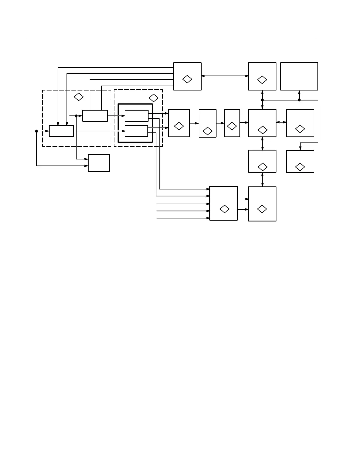
Figure 3–3: Aquisition system block diagram
Sampler Driver. The output of the attenuator drives the sampler driver inputs. The
sampler driver provides gain amplification, bandwidth limit filters, and outputs
for the sampler and trigger signal paths.
The sampler driver is an integrated circuit containing a differential input. The
sampler driver has a differential signal gain of 14X and a single-ended trigger
signal gain of 2X. The CPU controls the sampler driver bandwidth limit.
Sampler. The sampler provides two acquisition channels. It contains analog
acquisition memory and a heater circuit to provide temperature stabilization.
START/STOP tells the sampler when to start and stop acquiring data. ACQINIT
tells the sampler to prepare for a new acquisition.
Buffer Amp. The buffer amp converts the differential output signal of the sampler
to a single ended signal for use by the A/D converter.
A/D Converter. The A/D converter (U403) converts CH 1 and CH 2 analog
samples from the sampler to 8 bit digital values. The A/D reference voltage
is 1.0 V.
 Loading...