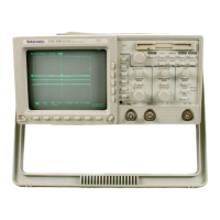
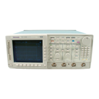
Theory of Operation
3–10
TDS 340A, TDS 360 & TDS 380 Technical Reference
charging and discharging currents are available at the collectors of Q304 and
Q305, respectively. The ratio of these currents is about 2000 to 1.
The trigger event initiates the charging ramp. The next occurrence of the system
clock disconnects the charging current, initiating the discharging ramp.
The baseline regulator circuit maintains the voltage at the collector of Q307 at 0
V while waiting for a trigger. When this node is at 0 V, the COUNTSTOP signal,
at the output of U304A, is low.
When U308B detects a trigger event at its input it sets ~RSTM to the “true” state,
which begins the fast ramp. Q307 is turned off so that the fast ramp charging
current will begin to charge the integration capacitors.
The constant current source, Q304 and associated components, determines the
fast charging rate. The charging current is nominally 22 mA through R302 and
Q304. This current flows through Q301 during the fast ramp charging time and
through Q302 during the slow ramp discharge time.
This fast ramp charging, initiated by the trigger event, will end when the next
system clock occurs. This causes the trigger logic (U309) to generate the
~RMSW and RMSW signals, to switch from fast-ramp charge to slow-ramp
discharge, and tells the TBC (U401) to start counting the ramp discharge time.
Q301 is now turned off (and Q302 turned on) to disconnect the 22 mA current
source from the integrating capacitors. Now the integrating capacitor discharges
through the 11 A current source formed by Q305 and associated components.
When the ramp crosses a –100 mV threshold, the COUNTSTOP signal goes
high, causing the TBC to stop the counting. This count represents the time from
trigger event until the next system clock. The circuitry reads the time base
interpolator counter, and then is reset by the next ACQINIT.
The signals ~RMST, RMST, ~RMSW, and RMSW are positive referenced ECL
levels. The COUNTSTOP signal has TTL levels.
Analog Trigger. The analog trigger is a free running analog comparator. It has a
variable input threshold determined by the TLM (trigger level).
The input has a channel switch. Control signals SR1, SR2, and SR3 select one of
five input signals. The channel switch output is at TP102. Probing this can
indicate whether or not the channel switch is working.
Once the source has been selected, filters can be applied to the signal. Filters
include high frequency reject, low frequency reject, DC coupled, AC coupled,
noise reject and AC noise reject.
Next, the signal is compared to a reference threshold (i.e., trigger level). The
polarity of the comparator can be switched to change the trigger slope. A shift
register controls filter selection, slope selection, and mode selection. The trigger
 Loading...