Do you have a question about the Texas Instruments C2000 LAUNCHXL-F280049C and is the answer not in the manual?
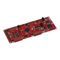
Highlights the key features of the F28004x LaunchPad, including MCU, debug probe, and expansion connectors.
Summarizes the technical specifications of the LAUNCHXL-F280049C board, including voltage and dimensions.
Describes the functional blocks and how peripherals interface with the MCU on the LaunchPad.
Describes the debug probe and serial communication interfaces for development.
Covers alternate routing of signals using switches for custom configurations and functionality.
Guides on programming the LaunchPad using the on-board XDS110 debug probe and CCS.
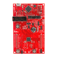
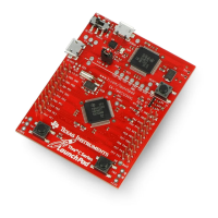
The C2000™ Piccolo™ F28004x Series LaunchPad™ Development Kit, specifically the LAUNCHXL-F280049C, is a low-cost development board designed for Texas Instruments' Piccolo F28004x series of microcontrollers (MCUs). This board is built around the TMS320F280049C MCU, highlighting its control, analog, and communications peripherals, as well as its integrated nonvolatile memory.
The primary function of the LaunchPad is to provide a versatile and cost-effective platform for developing applications with the F28004x series microcontrollers. It serves as an evaluation and development tool, enabling users to explore the capabilities of the MCU and integrate it into their custom circuits. The board is equipped with a comprehensive set of features to support various control applications, including motor control, and offers extensive expansion opportunities.
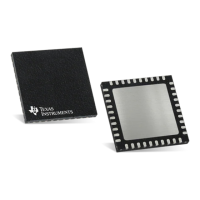
At its core, the F280049CPZS MCU is a 32-bit floating-point microcontroller operating at 100 MHz, featuring 256KB Flash memory and 100KB RAM. It includes advanced control peripherals, differentiated analog capabilities, and various communication peripherals, optimized for high-performance applications and designed for low-cost system solutions.
The LaunchPad comes factory-programmed with a quick start demo program residing in the on-chip Flash memory. This program executes every time power is applied, unless replaced by a user program. The demo utilizes the integrated Analog-to-Digital Converter (ADC) module to sample voltage on a pin and outputs the results via the Serial Communications Interface (SCI) Universal Asynchronous Receiver/Transmitter (UART) through the Virtual COM port (VCP) of the on-board XDS110 debug probe to a PC running a serial monitor.
The board features two independent BoosterPack XL expansion connectors, which are compliant with the BoosterPack standard, allowing for stackable headers to maximize expansion through the BoosterPack ecosystem. This enables users to connect a wide variety of add-on boards to extend the LaunchPad's functionality.
For debugging and programming, an on-board XDS110 debug probe is included. This probe supports 2-pin cJTAG mode, utilizing the TMS and TCK JTAG pins for programming and debugging the F280049C MCU using Code Composer Studio™ or other supported tool chains. The XDS110 also enumerates as a virtual COM port when connected to a USB host, facilitating serial communication with the MCU.
The LaunchPad supports various communication interfaces. It includes an on-board Controller Area Network (CAN) transceiver, allowing connection to a CAN network. Two independent Enhanced Quadrature Encoder Pulse (QEP)-based encoder connectors are provided for connecting linear or rotary incremental encoders, taking 5V signals and down-converting them to 3.3V for the MCU's eQEP modules. A separate Fast Serial Interface (FSI) connector is also available, enabling robust high-speed communications.
Power management is flexible, with selectable power domains from USB (isolated), BoosterPack connectors, or an external power supply. The board also includes a 5V step-up converter.
To begin using the F28004x LaunchPad, users should first follow the included README First document to run the pre-programmed quick start application. This allows for quick control and monitoring of the LaunchPad.
Experimentation with BoosterPacks is encouraged to expand the board's functionality. The two independent BoosterPack XL connectors allow for a variety of expansion opportunities, and users can find information on the TI LaunchPad web page for compatible BoosterPacks.
For developing custom control applications, the LaunchPad is supported by the C2000Ware development package. This package provides pre-configured example applications for the board, which can be used as a starting point for user projects. Users can also customize and integrate hardware to suit their specific end applications, using the LaunchPad as a reference for building custom circuits or as a foundation for expansion with custom BoosterPacks.
The board offers selectable power sources. By default, power is supplied via the connected USB. For applications requiring power isolation, jumpers JP1, JP2, and JP3 can be removed to isolate the USB from the MCU region, necessitating an external 3.3V supply to power the F280049C MCU and other on-board circuitry. Jumpers JP4, JP5, JP6, and JP7 provide additional connection points for external 3.3V or 5V supplies.
Alternate routing options for various GPIOs and peripherals are available through on-board switches or by manipulating 0Ω resistors. This allows users to configure the board to suit specific application needs, such as routing SCIA UART to the virtual COM port or to BoosterPack connectors, or enabling eQEP signals for encoders.
The FSI connector (J11) allows for loopback evaluation by adding two jumpers to connect TX to RX channels. For external board connections with FSI, each signal has an adjacent GND signal for wrapped-pair connections.
The board includes two user-controlled LEDs (LED4 red, LED5 green) connected to GPIO23 and GPIO34, respectively, which can be controlled by software applications. Two blue LEDs (LED2, LED3) indicate XDS110 debugger activity and are not software controllable. A microcontroller reset switch (S1) is also provided.
The LaunchPad is designed for ease of use and maintenance. The on-board XDS110 debug probe simplifies programming and debugging, eliminating the need for external debug tools in many cases.
The flexible power options, including USB isolation, allow for safe operation and debugging in high-voltage applications. When isolation is desired, removing the appropriate jumpers and providing an external power supply ensures safe operation.
The use of BoosterPack connectors promotes modularity and easy expansion. If two BoosterPacks are simultaneously connected and both provide power, jumper JP8 can be removed to isolate 3.3V and 5V from BoosterPack 2 headers, preventing power contention.
The analog voltage reference header (J15) allows for an external voltage source for VREFHIx, providing flexibility for the analog subsystem. While no signal conditioning circuitry is in place by default, users can add additional circuitry for best performance.
The design includes provisions for RC filters on PGA input signals, with 0Ω series resistors and pads for decoupling capacitors. These can be modified based on application requirements. An isolated ground plane for PGAs helps limit outside noise coupling, and the resistor connecting it to the PCB ground can be removed if isolation is needed.
The FSI to BoosterPack isolation resistors (R44, R45, R46, R47) can be removed to eliminate extended traces to BoosterPack headers, which helps limit noise or reflections when FSI toggles at high rates.
For GPIO18/X2, which is multiplexed with the oscillator clock output, R31 can be removed to separate GPIO18 from the on-board crystal oscillator (Y2), and R28 can be populated to connect GPIO18 to the BoosterPack connector, with R35 connecting X1 to Ground, if GPIO18 functionality is needed at the BoosterPack Connector.
The board's design, including the routing of microcontroller signals to 0.1-inch pitch headers, facilitates easy external circuitry connections. The internal multiplexer for GPIO pads allows for flexible assignment of peripheral functions, which can be configured as needed.
| Microcontroller | C2000 |
|---|---|
| Core Size | 32-Bit |
| Clock Speed | 100 MHz |
| RAM | 100KB |
| Operating Voltage | 3.3V |
| On-Board Debug Probe | Yes |
| Communication Interfaces | I2C, SPI, UART |
| Operating Temperature | -40°C ~ 125°C |
| Peripherals | Comparator, DAC |

