EasyManua.ls Logo

Texas Instruments MSP430F5529

Texas Instruments MSP430F5529
128 pages
To Next Page IconTo Next Page
Loading...
Product
Folder
Sample &
Buy
Technical
Documents
Tools &
Software
Support &
Community
Reference
Design
MSP430F5529
,
MSP430F5528
,
MSP430F5527
,
MSP430F5526
MSP430F5525
,
MSP430F5524
,
MSP430F5522
,
MSP430F5521
MSP430F5519, MSP430F5517, MSP430F5515, MSP430F5514, MSP430F5513
SLAS590M MARCH 2009REVISED NOVEMBER 2015
MSP430F552x, MSP430F551x Mixed-Signal Microcontrollers
1 Device Overview
1.1 Features
1
Low-Frequency Trimmed Internal Reference
Low Supply Voltage Range:
Source (REFO)
3.6 V Down to 1.8 V
32-kHz Watch Crystals (XT1)
Ultra-Low Power Consumption
High-Frequency Crystals up to 32 MHz (XT2)
Active Mode (AM):
16-Bit Timer TA0, Timer_A With Five
All System Clocks Active:
Capture/Compare Registers
290 µA/MHz at 8 MHz, 3.0 V, Flash
16-Bit Timer TA1, Timer_A With Three
Program Execution (Typical)
Capture/Compare Registers
150 µA/MHz at 8 MHz, 3.0 V, RAM
16-Bit Timer TA2, Timer_A With Three
Program Execution (Typical)
Capture/Compare Registers
Standby Mode (LPM3):
16-Bit Timer TB0, Timer_B With Seven
Real-Time Clock (RTC) With Crystal,
Capture/Compare Shadow Registers
Watchdog, and Supply Supervisor
Two Universal Serial Communication Interfaces
Operational, Full RAM Retention, Fast Wake
USCI_A0 and USCI_A1 Each Support:
up:
Enhanced UART Supports Automatic Baud-
1.9 µA at 2.2 V, 2.1 µA at 3.0 V (Typical)
Rate Detection
Low-Power Oscillator (VLO), General-
IrDA Encoder and Decoder
Purpose Counter, Watchdog, and Supply
Supervisor Operational, Full RAM Retention,
Synchronous SPI
Fast Wake up:
USCI_B0 and USCI_B1 Each Support:
1.4 µA at 3.0 V (Typical)
I
2
C
Off Mode (LPM4):
Synchronous SPI
Full RAM Retention, Supply Supervisor
Full-Speed Universal Serial Bus (USB)
Operational, Fast Wake up:
Integrated USB-PHY
1.1 µA at 3.0 V (Typical)
Integrated 3.3-V and 1.8-V USB Power System
Shutdown Mode (LPM4.5):
Integrated USB-PLL
0.18 µA at 3.0 V (Typical)
Eight Input and Eight Output Endpoints
Wake up From Standby Mode in 3.5 µs (Typical)
12-Bit Analog-to-Digital Converter (ADC)
16-Bit RISC Architecture, Extended Memory, up to
(MSP430F552x Only) With Internal Reference,
25-MHz System Clock
Sample-and-Hold, and Autoscan Feature
Flexible Power Management System
Comparator
Fully Integrated LDO With Programmable
Hardware Multiplier Supports 32-Bit Operations
Regulated Core Supply Voltage
Serial Onboard Programming, No External
Supply Voltage Supervision, Monitoring, and
Programming Voltage Needed
Brownout
Three-Channel Internal DMA
Unified Clock System
Basic Timer With RTC Feature
FLL Control Loop for Frequency Stabilization
Section 3 Summarizes Available Family Members
Low-Power Low-Frequency Internal Clock
For Complete Module Descriptions, See the
Source (VLO)
MSP430x5xx and MSP430x6xx Family User's
Guide (SLAU208)
1.2 Applications
Analog and Digital Sensor Systems Connection to USB Hosts
Data Loggers
1
An IMPORTANT NOTICE at the end of this data sheet addresses availability, warranty, changes, use in safety-critical applications,
intellectual property matters and other important disclaimers. PRODUCTION DATA.

Table of Contents

Question and Answer IconNeed help?

Do you have a question about the Texas Instruments MSP430F5529 and is the answer not in the manual?

Texas Instruments MSP430F5529 Specifications

General IconGeneral
Architecture16-bit RISC
CoreMSP430
Clock Speed25 MHz
Flash Memory128 KB
RAM8 KB
ADC12-bit
ADC Channels8
DAC Channels0
UART2
I2C1
SPI1
Operating Voltage1.8V - 3.6V
Operating Temperature-40°C to 85°C
Timers4 x 16-bit
PackageLQFP-64

Summary

1 Device Overview

1.1 Features

Lists key features of the microcontroller, including voltage range, power consumption, clocks, timers, and peripherals.

4 Terminal Configuration and Functions

4.2 Signal Descriptions

Provides a detailed list of device terminals, their functions, and their availability across different device variants and packages.

5 Specifications

5.1 Absolute Maximum Ratings

Specifies the absolute maximum operating conditions beyond which the device may be permanently damaged.

5.2 ESD Ratings

Details the electrostatic discharge sensitivity levels and ratings for the device according to industry standards.

5.3 Recommended Operating Conditions

Outlines the recommended operating conditions for supply voltage, temperature, and other parameters for reliable device operation.

5.5 Low-Power Mode Supply Currents (Into VCC) Excluding External Current

5.15 Crystal Oscillator, XT1, Low-Frequency Mode

5.16 Crystal Oscillator, XT2

5.19 DCO Frequency

5.20 PMM, Brown-Out Reset (BOR)

5.26 Wake-up Times From Low-Power Modes and Reset

5.32 USCI (SPI Master Mode)

5.33 USCI (SPI Slave Mode)

5.34 USCI (I2 C Mode)

5.35 12-Bit ADC, Power Supply and Input Range Conditions

5.41 REF, Built-In Reference

5.44 USB Output Ports DP and DM

5.46 USB-PWR (USB Power System)

5.48 Flash Memory

5.49 JTAG and Spy-Bi-Wire Interface

Specifies parameters for the JTAG and Spy-Bi-Wire interfaces, including input frequencies and pulse durations.

6 Detailed Description

6.1 CPU (Link to Users Guide)

Describes the MSP430 CPU architecture, registers, and instruction set capabilities.

6.2 Operating Modes

6.3 Interrupt Vector Addresses

6.4 Memory Organization

6.5 Bootstrap Loader (BSL)

6.6 JTAG Operation

6.7 Flash Memory (Link to Users Guide)

6.9 Peripherals

Provides an overview of the various peripheral modules available on the microcontroller.

6.9.1 Digital IO (Link to Users Guide)

6.9.2 Port Mapping Controller (Link to Users Guide)

6.9.3 Oscillator and System Clock (Link to Users Guide)

6.9.4 Power Management Module (PMM) (Link to Users Guide)

Details the Power Management Module (PMM), including its integrated voltage regulator, supply voltage supervisor (SVS), and monitor (SVM) circuitry.

6.9.8 System Module (SYS) (Link to Users Guide)

6.9.9 DMA Controller (Link to Users Guide)

6.9.10 Universal Serial Communication Interface (USCI) (Links to Users Guide: UART Mode, SPI Mode, I2 C Mode)

6.9.15 ComparatorB (Link to Users Guide)

6.9.19 Universal Serial Bus (USB) (Link to Users Guide)

Details the USB module, a fully integrated interface compliant with the USB 2.0 specification, including LDO, PHY, and PLL.

Table 6-37. DMA Registers (Base Address DMA General Control: 0500 h, DMA Channel 0: 0510 h, DMA Channel 1: 0520 h, DMA Channel 2: 0530 h)

Table 6-42. ADC12 A Registers (Base Address: 0700 h)

6.10 InputOutput Schematics

6.10.2 Port P2, P2.0 to P2.7, InputOutput With Schmitt Trigger

6.10.3 Port P3, P3.0 to P3.7, InputOutput With Schmitt Trigger

6.10.4 Port P4, P4.0 to P4.7, InputOutput With Schmitt Trigger

6.10.5 Port P5, P5.0 and P5.1, InputOutput With Schmitt Trigger

6.10.6 Port P5, P5.2, InputOutput With Schmitt Trigger

6.10.7 Port P5, P5.3, InputOutput With Schmitt Trigger

6.10.7.1 Port P5, P5.4 and P5.5 InputOutput With Schmitt Trigger

6.10.8 Port P5, P5.6 to P5.7, InputOutput With Schmitt Trigger

6.10.9 Port P6, P6.0 to P6.7, InputOutput With Schmitt Trigger

6.10.10 Port P7, P7.0 to P7.3, InputOutput With Schmitt Trigger

6.10.11 Port P7, P7.4 to P7.7, InputOutput With Schmitt Trigger

6.10.12 Port P8, P8.0 to P8.2, InputOutput With Schmitt Trigger

6.10.13 Port PU.0 DP, PU.1 DM, PUR USB Ports

6.10.14 Port J, J.0 JTAG Pin TDO, InputOutput With Schmitt Trigger or Output

7 Device and Documentation Support

7.1 Device Support

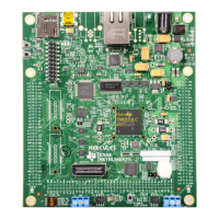
Provides an overview of device support, including getting started, tools, and hardware options.

7.1.2.3 Recommended Software Options

Lists recommended software options, including IDEs, MSPWare, TI-RTOS, USB Developer's Package, and programmer tools.

7.2 Documentation Support

Lists available documents such as User's Guides and Erratasheets for MSP430F552x and MSP430F551x devices.

8 Mechanical, Packaging, and Orderable Information

MECHANICAL DATA

Related product manuals