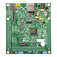
MSP430F5529
,
MSP430F5528
,
MSP430F5527
,
MSP430F5526
MSP430F5525
,
MSP430F5524
,
MSP430F5522
,
MSP430F5521
MSP430F5519, MSP430F5517, MSP430F5515, MSP430F5514, MSP430F5513
www.ti.com
SLAS590M –MARCH 2009–REVISED NOVEMBER 2015
Table of Contents
1 Device Overview ......................................... 1 5.24 PMM, SVS Low Side................................ 33
1.1 Features .............................................. 1 5.25 PMM, SVM Low Side ............................... 33
5.26 Wake-up Times From Low-Power Modes and
1.2 Applications........................................... 1
Reset ................................................ 34
1.3 Description............................................ 2
5.27 Timer_A ............................................. 34
1.4 Functional Block Diagrams........................... 3
5.28 Timer_B ............................................. 34
2 Revision History ......................................... 6
5.29 USCI (UART Mode) Clock Frequency .............. 35
3 Device Comparison ..................................... 7
5.30 USCI (UART Mode)................................. 35
4 Terminal Configuration and Functions.............. 8
5.31 USCI (SPI Master Mode) Clock Frequency......... 35
4.1 Pin Diagrams ......................................... 8
5.32 USCI (SPI Master Mode)............................ 35
4.2 Signal Descriptions.................................. 14
5.33 USCI (SPI Slave Mode)............................. 37
5 Specifications........................................... 19
5.34 USCI (I
2
C Mode) .................................... 39
5.1 Absolute Maximum Ratings ........................ 19
5.35 12-Bit ADC, Power Supply and Input Range
5.2 ESD Ratings ........................................ 19
Conditions ........................................... 40
5.3 Recommended Operating Conditions............... 19
5.36 12-Bit ADC, Timing Parameters .................... 40
5.4 Active Mode Supply Current Into V
CC
Excluding
5.37 12-Bit ADC, Linearity Parameters Using an External
External Current..................................... 21
Reference Voltage or AVCC as Reference Voltage 41
5.5 Low-Power Mode Supply Currents (Into V
CC
)
5.38 12-Bit ADC, Linearity Parameters Using the Internal
Excluding External Current.......................... 22
Reference Voltage .................................. 41
5.6 Thermal Characteristics............................. 23
5.39 12-Bit ADC, Temperature Sensor and Built-In V
MID
42
5.7 Schmitt-Trigger Inputs – General-Purpose I/O
5.40 REF, External Reference ........................... 43
(P1.0 to P1.7, P2.0 to P2.7, P3.0 to P3.7, P4.0 to P4.7)
(P5.0 to P5.7, P6.0 to P6.7, P7.0 to P7.7, P8.0 to
5.41 REF, Built-In Reference............................. 43
P8.2, PJ.0 to PJ.3, RST/NMI)....................... 24
5.42 Comparator_B....................................... 45
5.8 Inputs – Ports P1 and P2
5.43 Ports PU.0 and PU.1................................ 45
(P1.0 to P1.7, P2.0 to P2.7)......................... 24
5.44 USB Output Ports DP and DM...................... 47
5.9 Leakage Current – General-Purpose I/O
5.45 USB Input Ports DP and DM........................ 47
(P1.0 to P1.7, P2.0 to P2.7, P3.0 to P3.7, P4.0 to P4.7)
(P5.0 to P5.7, P6.0 to P6.7, P7.0 to P7.7, P8.0 to
5.46 USB-PWR (USB Power System) ................... 48
P8.2, PJ.0 to PJ.3, RST/NMI)....................... 24
5.47 USB-PLL (USB Phase Locked Loop)............... 48
5.10 Outputs – General-Purpose I/O (Full Drive Strength)
5.48 Flash Memory ....................................... 49
(P1.0 to P1.7, P2.0 to P2.7, P3.0 to P3.7, P4.0 to P4.7)
(P5.0 to P5.7, P6.0 to P6.7, P7.0 to P7.7, P8.0 to 5.49 JTAG and Spy-Bi-Wire Interface.................... 49
P8.2, PJ.0 to PJ.3) .................................. 24
6 Detailed Description ................................... 50
5.11 Outputs – General-Purpose I/O (Reduced Drive
6.1 CPU (Link to User's Guide) ......................... 50
Strength)
6.2 Operating Modes.................................... 51
(P1.0 to P1.7, P2.0 to P2.7, P3.0 to P3.7, P4.0 to P4.7)
(P5.0 to P5.7, P6.0 to P6.7, P7.0 to P7.7, P8.0 to
6.3 Interrupt Vector Addresses.......................... 52
P8.2, PJ.0 to PJ.3) .................................. 25
6.4 Memory Organization ............................... 53
5.12 Output Frequency – General-Purpose I/O
6.5 Bootstrap Loader (BSL) ............................. 54
(P1.0 to P1.7, P2.0 to P2.7, P3.0 to P3.7, P4.0 to P4.7)
6.6 JTAG Operation ..................................... 55
(P5.0 to P5.7, P6.0 to P6.7, P7.0 to P7.7, P8.0 to
P8.2, PJ.0 to PJ.3) .................................. 25
6.7 Flash Memory (Link to User's Guide)............... 56
5.13 Typical Characteristics – Outputs, Reduced Drive
6.8 RAM (Link to User's Guide)......................... 56
Strength (PxDS.y = 0)............................... 26
6.9 Peripherals .......................................... 56
5.14 Typical Characteristics – Outputs, Full Drive
6.10 Input/Output Schematics ............................ 81
Strength (PxDS.y = 1)............................... 27
6.11 Device Descriptors (TLV) .......................... 103
5.15 Crystal Oscillator, XT1, Low-Frequency Mode ..... 28
7 Device and Documentation Support.............. 109
5.16 Crystal Oscillator, XT2 .............................. 29
7.1 Device Support..................................... 109
5.17 Internal Very-Low-Power Low-Frequency Oscillator
7.2 Documentation Support............................ 112
(VLO) ................................................ 30
5.18 Internal Reference, Low-Frequency Oscillator
7.3 Related Links ...................................... 113
(REFO) .............................................. 30
7.4 Community Resources............................. 113
5.19 DCO Frequency..................................... 31
7.5 Trademarks ........................................ 113
5.20 PMM, Brown-Out Reset (BOR) ..................... 32
7.6 Electrostatic Discharge Caution ................... 113
5.21 PMM, Core Voltage ................................. 32
7.7 Glossary............................................ 113
5.22 PMM, SVS High Side ............................... 32
8 Mechanical, Packaging, and Orderable
5.23 PMM, SVM High Side............................... 33
Information............................................. 114
Copyright © 2009–2015, Texas Instruments Incorporated Table of Contents 5
Submit Documentation Feedback
Product Folder Links: MSP430F5529 MSP430F5528 MSP430F5527 MSP430F5526 MSP430F5525 MSP430F5524
MSP430F5522 MSP430F5521 MSP430F5519 MSP430F5517 MSP430F5515 MSP430F5514 MSP430F5513