Unified
Clock
System
128KB
96KB
64KB
32KB
Flash
8KB+2KB
6KB+2KB
4KB+2KB
RAM
MCLK
ACLK
SMCLK
I/OPorts
P1/P2
2×8I/Os
Interrupt
&Wakeup
PA
1×16I/Os
CPUXV2
and
Working
Registers
EEM
(L:8+2)
XIN
XOUT
JTAG/
Interface
SBW
PA PB PC
DMA
3Channel
XT2IN
XT OUT2
Power
Management
LDO
SVM/
Brownout
SVS
SYS
Watchdog
PortMap
Control
(P4)
I/OPorts
P3/P4
1×5I/Os
1
PB
1×13I/Os
×8I/Os
I/OPorts
P5/P6
1×6I/Os
PC
1×14I/Os
1×8I/Os
Full-speed
USB
USB-PHY
USB-LDO
USB-PLL
MPY32
TA0
Timer_A
5CC
Registers
TA1
Timer_A
3CC
Registers
TB0
Timer_B
7CC
Registers
RTC_A
CRC16
USCI0,1
USCI_Ax:
UART,
IrDA,SPI
USCI_Bx:
SPI,I2C
ADC12_A
200KSPS
12Channels
(10ext/2int)
Autoscan
12Bit
DVCC DVSS AVCC AVSS
P1.x P2.x
P3.x
P4.x
P5.x P6.x
DP,DM,PUR
RST/NMI
TA2
Timer_A
3CC
Registers
REF
VCORE
MAB
MDB
COMP_B
8Channels
Unified
Clock
System
128KB
96KB
64KB
32KB
Flash
8KB+2KB
6KB+2KB
4KB+2KB
RAM
MCLK
ACLK
SMCLK
I/OPorts
P1/P2
2×8I/Os
Interrupt
&Wakeup
PA
1×16I/Os
CPUXV2
and
Working
Registers
EEM
(L:8+2)
XIN
XOUT
JTAG/
Interface
SBW
PA PB PC PD
DMA
3Channel
XT2IN
XT OUT2
Power
Management
LDO
SVM/
Brownout
SVS
SYS
Watchdog
PortMap
Control
(P4)
I/OPorts
P3/P4
2×8I/Os
PB
1×16I/Os
I/OPorts
P5/P6
2×8I/Os
PC
1×16I/Os
I/OPorts
P7/P8
1×8I/Os
1
PD
1×11I/Os
×3I/Os
Full-speed
USB
USB-PHY
USB-LDO
USB-PLL
MPY32
TA0
Timer_A
5CC
Registers
TA1
Timer_A
3CC
Registers
TB0
Timer_B
7CC
Registers
RTC_A
CRC16
USCI0,1
USCI_Ax:
UART,
IrDA,SPI
USCI_Bx:
SPI,I2C
ADC12_A
200KSPS
16Channels
(14ext/2int)
Autoscan
12Bit
DVCC DVSS AVCC AVSS
P1.x P2.x
P3.x
P4.x
P5.x P6.x
DP,DM,PUR
RST/NMI
TA2
Timer_A
3CC
Registers
REF
VCORE
MAB
MDB
P7.x P8.x
COMP_B
12Channels
MSP430F5529
,
MSP430F5528
,
MSP430F5527
,
MSP430F5526
MSP430F5525
,
MSP430F5524
,
MSP430F5522
,
MSP430F5521
MSP430F5519, MSP430F5517, MSP430F5515, MSP430F5514, MSP430F5513
www.ti.com
SLAS590M –MARCH 2009–REVISED NOVEMBER 2015
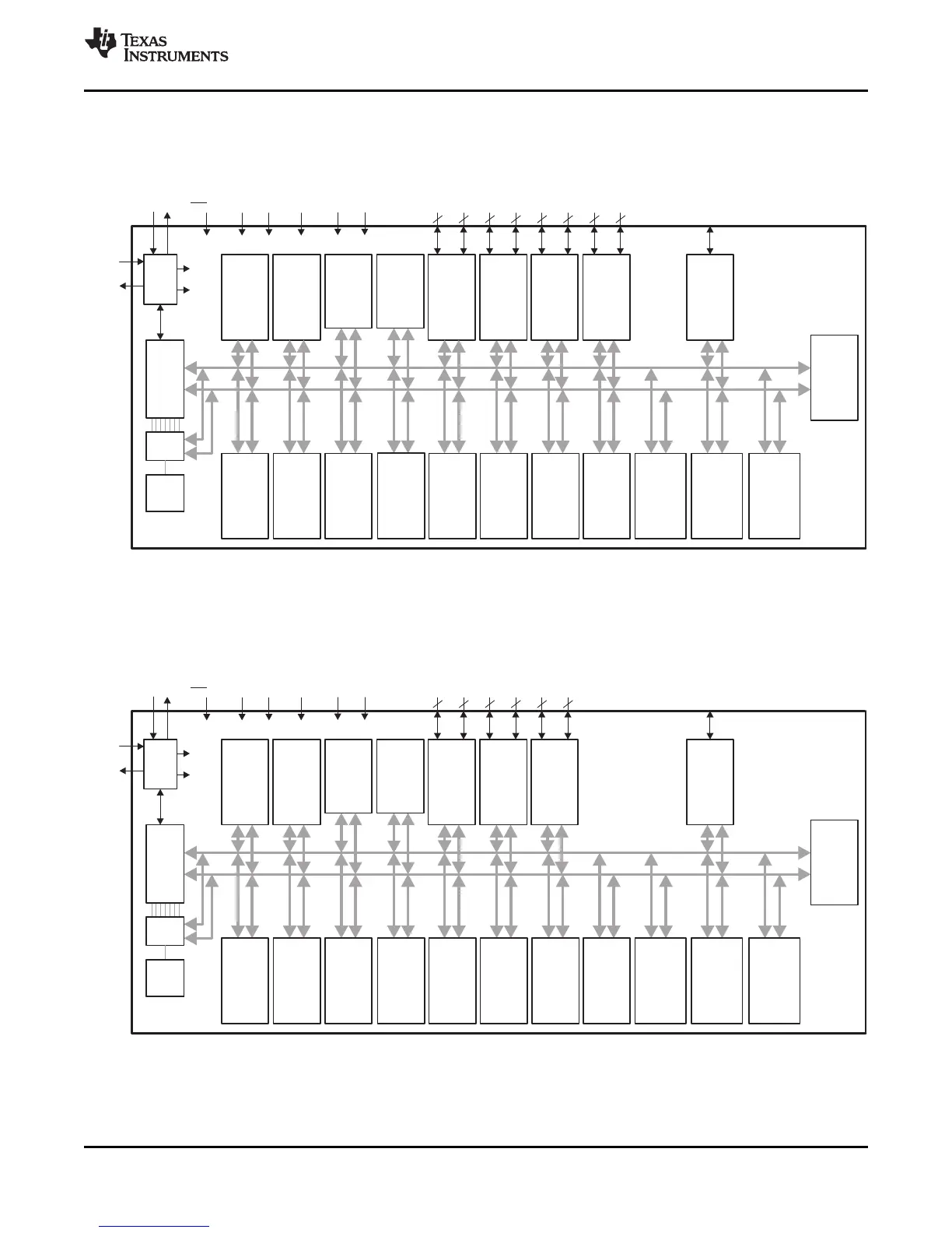
1.4 Functional Block Diagrams
Figure 1-1 shows the functional block diagram for the MSP430F5529, MSP430F5527, MSP430F5525, and
MSP430F5521 devices in the PN package.
Figure 1-1. Functional Block Diagram – MSP430F5529IPN, MSP430F5527IPN, MSP430F5525IPN,
MSP430F5521IPN
Figure 1-2 shows the functional block diagram for the MSP430F5528, MSP430F5526, MSP430F5524, and
MSP430F5522 devices in the RGC and ZQE packages and for the MSP430F5528, MSP430F5526, and
MSP430F5524 devices in the YFF package.
Figure 1-2. Functional Block Diagram –
MSP430F5528IRGC, MSP430F5526IRGC, MSP430F5524IRGC, MSP430F5522IRGC
MSP430F5528IZQE, MSP430F5526IZQE, MSP430F5524IZQE, MSP430F5522IZQE
MSP430F5528IYFF, MSP430F5526IYFF, MSP430F5524IYFF
Copyright © 2009–2015, Texas Instruments Incorporated Device Overview 3
Submit Documentation Feedback
Product Folder Links: MSP430F5529 MSP430F5528 MSP430F5527 MSP430F5526 MSP430F5525 MSP430F5524
MSP430F5522 MSP430F5521 MSP430F5519 MSP430F5517 MSP430F5515 MSP430F5514 MSP430F5513