MSP430F5529
,
MSP430F5528
,
MSP430F5527
,
MSP430F5526
MSP430F5525
,
MSP430F5524
,
MSP430F5522
,
MSP430F5521
MSP430F5519, MSP430F5517, MSP430F5515, MSP430F5514, MSP430F5513
www.ti.com
SLAS590M –MARCH 2009–REVISED NOVEMBER 2015
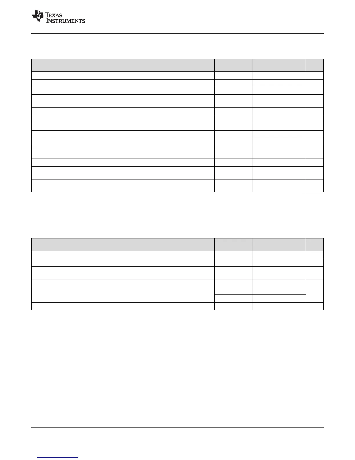
5.48 Flash Memory
over recommended ranges of supply voltage and operating free-air temperature (unless otherwise noted)
TEST
PARAMETER MIN TYP MAX UNIT
CONDITIONS
DV
CC(PGM,ERASE)
Program and erase supply voltage 1.8 3.6 V
I
PGM
Average supply current from DVCC during program
(1)
3 5 mA
I
ERASE
Average supply current from DVCC during erase
(1)
6 11 mA
Average supply current from DVCC during mass erase or bank
I
MERASE
, I
BANK
6 11 mA
erase
(1)
t
CPT
Cumulative program time See
(2)
16 ms
Program and erase endurance 10
4
10
5
cycles
t
Retention
Data retention duration T
J
= 25°C 100 years
t
Word
Word or byte program time See
(3)
64 85 µs
t
Block, 0
Block program time for first byte or word See
(3)
49 65 µs
Block program time for each additional byte or word, except for last
t
Block, 1–(N–1)
See
(3)
37 49 µs
byte or word
t
Block, N
Block program time for last byte or word See
(3)
55 73 µs
Erase time for segment, mass erase, and bank erase when
t
Erase
See
(3)
23 32 ms
available.
MCLK frequency in marginal read mode
f
MCLK,MRG
0 1 MHz
(FCTL4.MRG0 = 1 or FCTL4.MRG1 = 1)
(1) Default clock system frequency of MCLK = 1 MHz, ACLK = 32768 Hz, SMCLK = 1 MHz. No peripherals are enabled or active.
(2) The cumulative program time must not be exceeded when writing to a 128-byte flash block. This parameter applies to all programming
methods: individual word- or byte-write and block-write modes.
(3) These values are hardwired into the state machine of the flash controller.
5.49 JTAG and Spy-Bi-Wire Interface
over recommended ranges of supply voltage and operating free-air temperature (unless otherwise noted)
TEST
PARAMETER MIN TYP MAX UNIT
CONDITIONS
f
SBW
Spy-Bi-Wire input frequency 2.2 V, 3 V 0 20 MHz
t
SBW,Low
Spy-Bi-Wire low clock pulse duration 2.2 V, 3 V 0.025 15 µs
Spy-Bi-Wire enable time (TEST high to acceptance of first clock
t
SBW, En
2.2 V, 3 V 1 µs
edge)
(1)
t
SBW,Rst
Spy-Bi-Wire return to normal operation time 15 100 µs
2.2 V 0 5
f
TCK
TCK input frequency, 4-wire JTAG
(2)
MHz
3 V 0 10
R
internal
Internal pulldown resistance on TEST 2.2 V, 3 V 45 60 80 kΩ
(1) Tools that access the Spy-Bi-Wire interface must wait for the t
SBW,En
time after pulling the TEST/SBWTCK pin high before applying the
first SBWTCK clock edge.
(2) f
TCK
may be restricted to meet the timing requirements of the module selected.
Copyright © 2009–2015, Texas Instruments Incorporated Specifications 49
Submit Documentation Feedback
Product Folder Links: MSP430F5529 MSP430F5528 MSP430F5527 MSP430F5526 MSP430F5525 MSP430F5524
MSP430F5522 MSP430F5521 MSP430F5519 MSP430F5517 MSP430F5515 MSP430F5514 MSP430F5513