MSP430F5529
,
MSP430F5528
,
MSP430F5527
,
MSP430F5526
MSP430F5525
,
MSP430F5524
,
MSP430F5522
,
MSP430F5521
MSP430F5519, MSP430F5517, MSP430F5515, MSP430F5514, MSP430F5513
www.ti.com
SLAS590M –MARCH 2009–REVISED NOVEMBER 2015
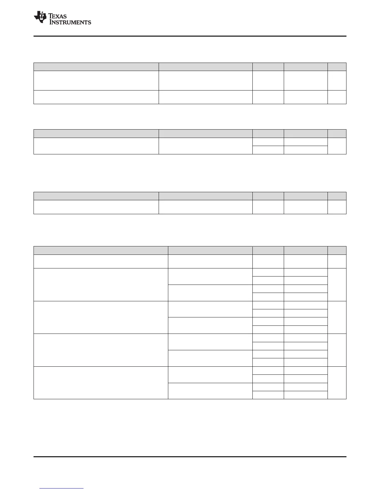
5.29 USCI (UART Mode) Clock Frequency
over recommended ranges of supply voltage and operating free-air temperature (unless otherwise noted)
PARAMETER CONDITIONS V
CC
MIN MAX UNIT
Internal: SMCLK, ACLK,
f
USCI
USCI input clock frequency External: UCLK, f
SYSTEM
MHz
Duty cycle = 50% ± 10%
BITCLK clock frequency
f
BITCLK
1 MHz
(equals baud rate in MBaud)
5.30 USCI (UART Mode)
over recommended ranges of supply voltage and operating free-air temperature (unless otherwise noted)
PARAMETER TEST CONDITIONS V
CC
MIN MAX UNIT
2.2 V 50 600
t
t
UART receive deglitch time
(1)
ns
3 V 50 600
(1) Pulses on the UART receive input (UCxRX) shorter than the UART receive deglitch time are suppressed. To ensure that pulses are
correctly recognized, their duration should exceed the maximum specification of the deglitch time.
5.31 USCI (SPI Master Mode) Clock Frequency
over recommended ranges of supply voltage and operating free-air temperature (unless otherwise noted)
PARAMETER CONDITIONS V
CC
MIN MAX UNIT
Internal: SMCLK, ACLK,
f
USCI
USCI input clock frequency f
SYSTEM
MHz
Duty cycle = 50% ± 10%
5.32 USCI (SPI Master Mode)
over recommended ranges of supply voltage and operating free-air temperature (unless otherwise noted)
(1)
(see Figure 5-11 and Figure 5-12)
PARAMETER TEST CONDITIONS V
CC
MIN MAX UNIT
SMCLK, ACLK,
f
USCI
USCI input clock frequency f
SYSTEM
MHz
Duty cycle = 50% ± 10%
1.8 V 55
PMMCOREV = 0
3.0 V 38
t
SU,MI
SOMI input data setup time ns
2.4 V 30
PMMCOREV = 3
3.0 V 25
1.8 V 0
PMMCOREV = 0
3.0 V 0
t
HD,MI
SOMI input data hold time ns
2.4 V 0
PMMCOREV = 3
3.0 V 0
1.8 V 20
UCLK edge to SIMO valid,
C
L
= 20 pF, PMMCOREV = 0
3.0 V 18
t
VALID,MO
SIMO output data valid time
(2)
ns
2.4 V 16
UCLK edge to SIMO valid,
C
L
= 20 pF, PMMCOREV = 3
3.0 V 15
1.8 V –10
C
L
= 20 pF, PMMCOREV = 0
3.0 V –8
t
HD,MO
SIMO output data hold time
(3)
ns
2.4 V –10
C
L
= 20 pF, PMMCOREV = 3
3.0 V –8
(1) f
UCxCLK
= 1/2t
LO/HI
with t
LO/HI
≥ max(t
VALID,MO(USCI)
+ t
SU,SI(Slave)
, t
SU,MI(USCI)
+ t
VALID,SO(Slave)
).
For the slave parameters t
SU,SI(Slave)
and t
VALID,SO(Slave)
, see the SPI parameters of the attached slave.
(2) Specifies the time to drive the next valid data to the SIMO output after the output changing UCLK clock edge. See the timing diagrams
in Figure 5-11 and Figure 5-12.
(3) Specifies how long data on the SIMO output is valid after the output changing UCLK clock edge. Negative values indicate that the data
on the SIMO output can become invalid before the output changing clock edge observed on UCLK. See the timing diagrams in Figure 5-
11 and Figure 5-12.
Copyright © 2009–2015, Texas Instruments Incorporated Specifications 35
Submit Documentation Feedback
Product Folder Links: MSP430F5529 MSP430F5528 MSP430F5527 MSP430F5526 MSP430F5525 MSP430F5524
MSP430F5522 MSP430F5521 MSP430F5519 MSP430F5517 MSP430F5515 MSP430F5514 MSP430F5513