MSP430F5529
,
MSP430F5528
,
MSP430F5527
,
MSP430F5526
MSP430F5525
,
MSP430F5524
,
MSP430F5522
,
MSP430F5521
MSP430F5519, MSP430F5517, MSP430F5515, MSP430F5514, MSP430F5513
SLAS590M –MARCH 2009–REVISED NOVEMBER 2015
www.ti.com
4.2 Signal Descriptions
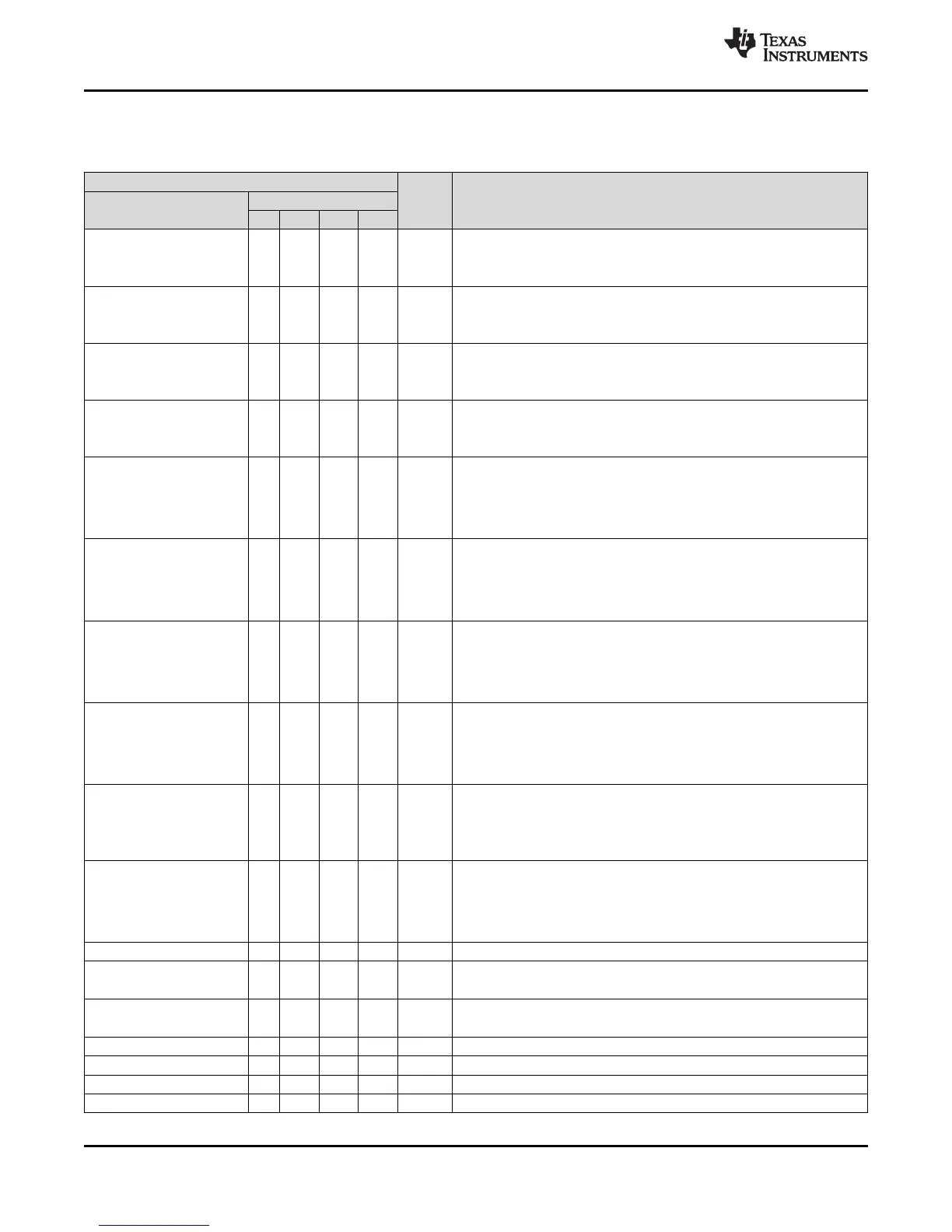
Table 4-1. Terminal Functions
TERMINAL
NO. I/O
(1)
DESCRIPTION
NAME
PN RGC YFF ZQE
General-purpose digital I/O
P6.4/CB4/A4 1 5 B2 C1 I/O Comparator_B input CB4
Analog input A4 – ADC (not available on F551x devices)
General-purpose digital I/O
P6.5/CB5/A5 2 6 B3 D2 I/O Comparator_B input CB5
Analog input A5 – ADC (not available on F551x devices)
General-purpose digital I/O
P6.6/CB6/A6 3 7 A2 D1 I/O Comparator_B input CB6
Analog input A6 – ADC (not available on F551x devices)
General-purpose digital I/O
P6.7/CB7/A7 4 8 C5 D3 I/O Comparator_B input CB7
Analog input A7 – ADC (not available on F551x devices)
General-purpose digital I/O (not available on F5528, F5526, F5524, F5522, F5514,
F5513 devices)
P7.0/CB8/A12 5 N/A N/A N/A I/O Comparator_B input CB8 (not available on F5528, F5526, F5524, F5522, F5514,
F5513 devices)
Analog input A12 – ADC (not available on F551x devices)
General-purpose digital I/O (not available on F5528, F5526, F5524, F5522, F5514,
F5513 devices)
P7.1/CB9/A13 6 N/A N/A N/A I/O Comparator_B input CB9 (not available on F5528, F5526, F5524, F5522, F5514,
F5513 devices)
Analog input A13 – ADC (not available on F551x devices)
General-purpose digital I/O (not available on F5528, F5526, F5524, F5522, F5514,
F5513 devices)
P7.2/CB10/A14 7 N/A N/A N/A I/O Comparator_B input CB10 (not available on F5528, F5526, F5524, F5522, F5514,
F5513 devices)
Analog input A14 – ADC (not available on F551x devices)
General-purpose digital I/O (not available on F5528, F5526, F5524, F5522, F5514,
F5513 devices)
P7.3/CB11/A15 8 N/A N/A N/A I/O Comparator_B input CB11 (not available on F5528, F5526, F5524, F5522, F5514,
F5513 devices)
Analog input A15 – ADC (not available on F551x devices)
General-purpose digital I/O
Output of reference voltage to the ADC (not available on F551x devices)
P5.0/A8/VREF+/VeREF+ 9 9 B4 E1 I/O
Input for an external reference voltage to the ADC (not available on F551x devices)
Analog input A8 – ADC (not available on F551x devices)
General-purpose digital I/O
Negative terminal for the ADC reference voltage for both sources, the internal
P5.1/A9/VREF-/VeREF- 10 10 B5 E2 I/O reference voltage, or an external applied reference voltage (not available on F551x
devices)
Analog input A9 – ADC (not available on F551x devices)
AVCC1 11 11 A3 F2 Analog power supply
General-purpose digital I/O
P5.4/XIN 12 12 A5 F1 I/O
Input terminal for crystal oscillator XT1
General-purpose digital I/O
P5.5/XOUT 13 13 A6 G1 I/O
Output terminal of crystal oscillator XT1
AVSS1 14 14 A4 G2 Analog ground supply
P8.0 15 N/A N/A N/A I/O General-purpose digital I/O
P8.1 16 N/A N/A N/A I/O General-purpose digital I/O
P8.2 17 N/A N/A N/A I/O General-purpose digital I/O
(1) I = input, O = output, N/A = not available
14 Terminal Configuration and Functions Copyright © 2009–2015, Texas Instruments Incorporated
Submit Documentation Feedback
Product Folder Links: MSP430F5529 MSP430F5528 MSP430F5527 MSP430F5526 MSP430F5525 MSP430F5524
MSP430F5522 MSP430F5521 MSP430F5519 MSP430F5517 MSP430F5515 MSP430F5514 MSP430F5513