MSP430F5529
,
MSP430F5528
,
MSP430F5527
,
MSP430F5526
MSP430F5525
,
MSP430F5524
,
MSP430F5522
,
MSP430F5521
MSP430F5519, MSP430F5517, MSP430F5515, MSP430F5514, MSP430F5513
www.ti.com
SLAS590M –MARCH 2009–REVISED NOVEMBER 2015
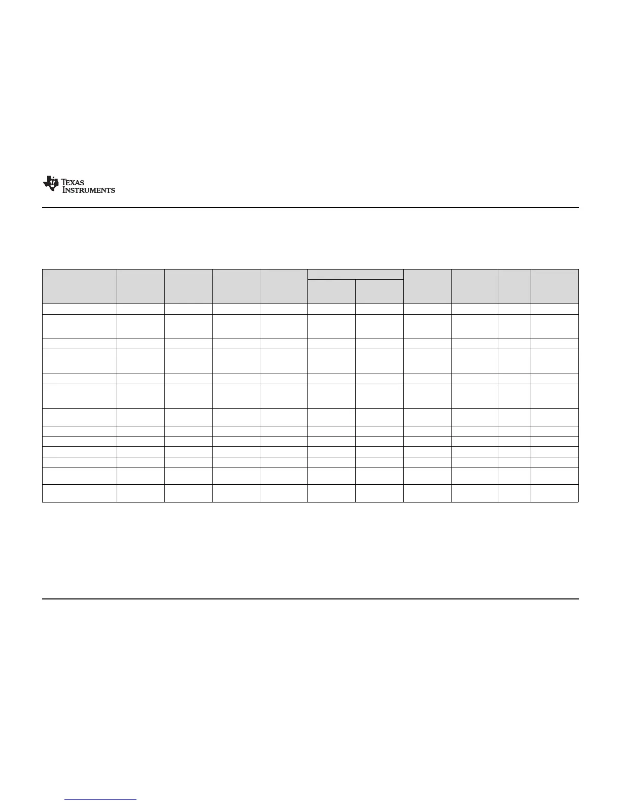
3 Device Comparison
Table 3-1 summarizes the available family members.
Table 3-1. Family Members
(1)(2)
USCI
FLASH SRAM ADC12_A Comp_B
CHANNEL A: CHANNEL B:
DEVICE Timer_A
(4)
Timer_B
(5)
I/O PACKAGE
(KB) (KB)
(3)
(Ch) (Ch)
UART, IrDA, SPI, I
2
C
SPI
MSP430F5529 128 8 + 2 5, 3, 3 7 2 2 14 ext, 2 int 12 63 80 PN
64 RGC,
MSP430F5528 128 8 + 2 5, 3, 3 7 2 2 10 ext, 2 int 8 47 64 YFF,
80 ZQE
MSP430F5527 96 6 + 2 5, 3, 3 7 2 2 14 ext, 2 int 12 63 80 PN
64 RGC,
MSP430F5526 96 6 + 2 5, 3, 3 7 2 2 10 ext, 2 int 8 47 64 YFF,
80 ZQE
MSP430F5525 64 4 + 2 5, 3, 3 7 2 2 14 ext, 2 int 12 63 80 PN
64 RGC,
MSP430F5524 64 4 + 2 5, 3, 3 7 2 2 10 ext, 2 int 8 47 64 YFF,
80 ZQE
64 RGC,
MSP430F5522 32 8 + 2 5, 3, 3 7 2 2 10 ext, 2 int 8 47
80 ZQE
MSP430F5521 32 6 + 2 5, 3, 3 7 2 2 14 ext, 2 int 12 63 80 PN
MSP430F5519 128 8 + 2 5, 3, 3 7 2 2 – 12 63 80 PN
MSP430F5517 96 6 + 2 5, 3, 3 7 2 2 – 12 63 80 PN
MSP430F5515 64 4 + 2 5, 3, 3 7 2 2 – 12 63 80 PN
64 RGC,
MSP430F5514 64 4 + 2 5, 3, 3 7 2 2 – 8 47
80 ZQE
64 RGC,
MSP430F5513 32 4 + 2 5, 3, 3 7 2 2 – 8 47
80 ZQE
(1) For the most current part, package, and ordering information for all available devices, see the Package Option Addendum in Section 8, or see the TI website at www.ti.com.
(2) Package drawings, thermal data, and symbolization are available at www.ti.com/packaging.
(3) The additional 2KB USB SRAM that is listed can be used as general-purpose SRAM when USB is not in use.
(4) Each number in the sequence represents an instantiation of Timer_A with its associated number of capture/compare registers and PWM output generators available. For example, a
number sequence of 3, 5 would represent two instantiations of Timer_A, the first instantiation having 3 and the second instantiation having 5 capture/compare registers and PWM output
generators, respectively.
(5) Each number in the sequence represents an instantiation of Timer_B with its associated number of capture/compare registers and PWM output generators available. For example, a
number sequence of 3, 5 would represent two instantiations of Timer_B, the first instantiation having 3 and the second instantiation having 5 capture/compare registers and PWM output
generators, respectively.
Copyright © 2009–2015, Texas Instruments Incorporated Device Comparison 7
Submit Documentation Feedback
Product Folder Links: MSP430F5529 MSP430F5528 MSP430F5527 MSP430F5526 MSP430F5525 MSP430F5524
MSP430F5522 MSP430F5521 MSP430F5519 MSP430F5517 MSP430F5515 MSP430F5514 MSP430F5513