Unified
Clock
System
64KB
32KB
Flash
4KB+2KB
RAM
MCLK
ACLK
SMCLK
I/O Ports
P1/P2
2×8 I/Os
Interrupt
& Wakeup
PA
1×16 I/Os
CPUXV2
and
Working
Registers
EEM
(L: 8+2)
XIN
XOUT
JTAG/
SBW
Interface
PA PB PC
DMA
3 Channel
XT2IN
XT2OUT
Power
Management
LDO
SVM/SVS
Brownout
SYS
Watchdog
Port Map
Control
(P4)
I/O Ports
P3/P4
1×5 I/Os
1
PB
1×13 I/Os
×8 I/Os
I/O Ports
P5/P6
1×6 I/Os
PC
1×14 I/Os
1×8 I/Os
Full-speed
USB
USB-PHY
USB-LDO
USB-PLL
MPY32
TA0
Timer_A
5 CC
Registers
TA1
Timer_A
3 CC
Registers
TB0
Timer_B
7 CC
Registers
RTC_A
CRC16
USCI0,1
USCI_Ax:
UART,
IrDA, SPI
USCI_Bx:
SPI, I2C
DVCC DVSS AVCC AVSS
P1.x P2.x
P3.x
P4.x
P5.x P6.x
DP,DM,PUR
RST/NMI
TA2
Timer_A
3 CC
Registers
COMP_B
8 Channels
VCORE
MAB
MDB
REF
Unified
Clock
System
128KB
96KB
64KB
Flash
4KB+2KB
RAM
MCLK
ACLK
SMCLK
I/O Ports
P1/P2
2×8 I/Os
Interrupt
& Wakeup
PA
1×16 I/Os
CPUXV2
and
Working
Registers
EEM
(L: 8+2)
XIN
XOUT
JTAG/
SBW
Interface
PA PB PC PD
DMA
3 Channel
XT2IN
XT2OUT
Power
Management
LDO
SVM/SVS
Brownout
SYS
Watchdog
Port Map
Control
(P4)
I/O Ports
P3/P4
2×8 I/Os
PB
1×16 I/Os
I/O Ports
P5/P6
2×8 I/Os
PC
1×16 I/Os
I/O Ports
P7/P8
1×8 I/Os
1
PD
1×11 I/Os
×3 I/Os
Full-speed
USB
USB-PHY
USB-LDO
USB-PLL
MPY32
TA0
Timer_A
5 CC
Registers
TA1
Timer_A
3 CC
Registers
TB0
Timer_B
7 CC
Registers
RTC_A
CRC16
USCI0,1
USCI_Ax:
UART,
IrDA, SPI
USCI_Bx:
SPI, I2C
DVCC DVSS AVCC AVSS
P1.x P2.x
P3.x
P4.x
P5.x P6.x
DP,DM,PUR
RST/NMI
TA2
Timer_A
3 CC
Registers
COMP_B
12 Channels
VCORE
MAB
MDB
P7.x P8.x
REF
MSP430F5529
,
MSP430F5528
,
MSP430F5527
,
MSP430F5526
MSP430F5525
,
MSP430F5524
,
MSP430F5522
,
MSP430F5521
MSP430F5519, MSP430F5517, MSP430F5515, MSP430F5514, MSP430F5513
SLAS590M –MARCH 2009–REVISED NOVEMBER 2015
www.ti.com
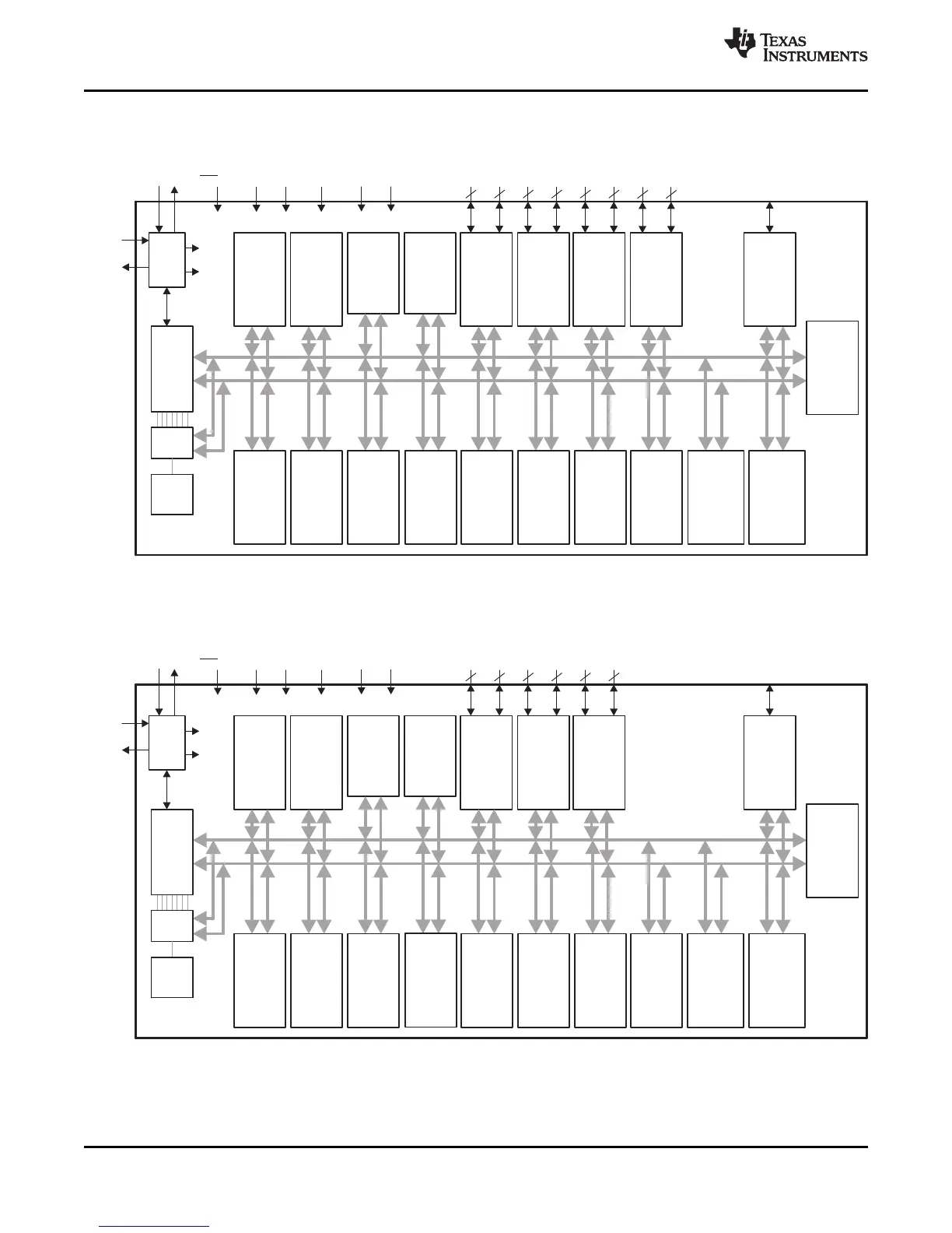
Figure 1-3 shows the functional block diagram for the MSP430F5519, MSP430F5517, and MSP430F5515
devices in the PN package.
Figure 1-3. Functional Block Diagram – MSP430F5519IPN, MSP430F5517IPN, MSP430F5515IPN
Figure 1-4 shows the functional block diagram for the MSP430F5514 and MSP430F5513 devices in the
RGC and ZQE packages.
Figure 1-4. Functional Block Diagram – MSP430F5514IRGC, MSP430F5513IRGC, MSP430F5514IZQE,
MSP430F5513IZQE
4 Device Overview Copyright © 2009–2015, Texas Instruments Incorporated
Submit Documentation Feedback
Product Folder Links: MSP430F5529 MSP430F5528 MSP430F5527 MSP430F5526 MSP430F5525 MSP430F5524
MSP430F5522 MSP430F5521 MSP430F5519 MSP430F5517 MSP430F5515 MSP430F5514 MSP430F5513