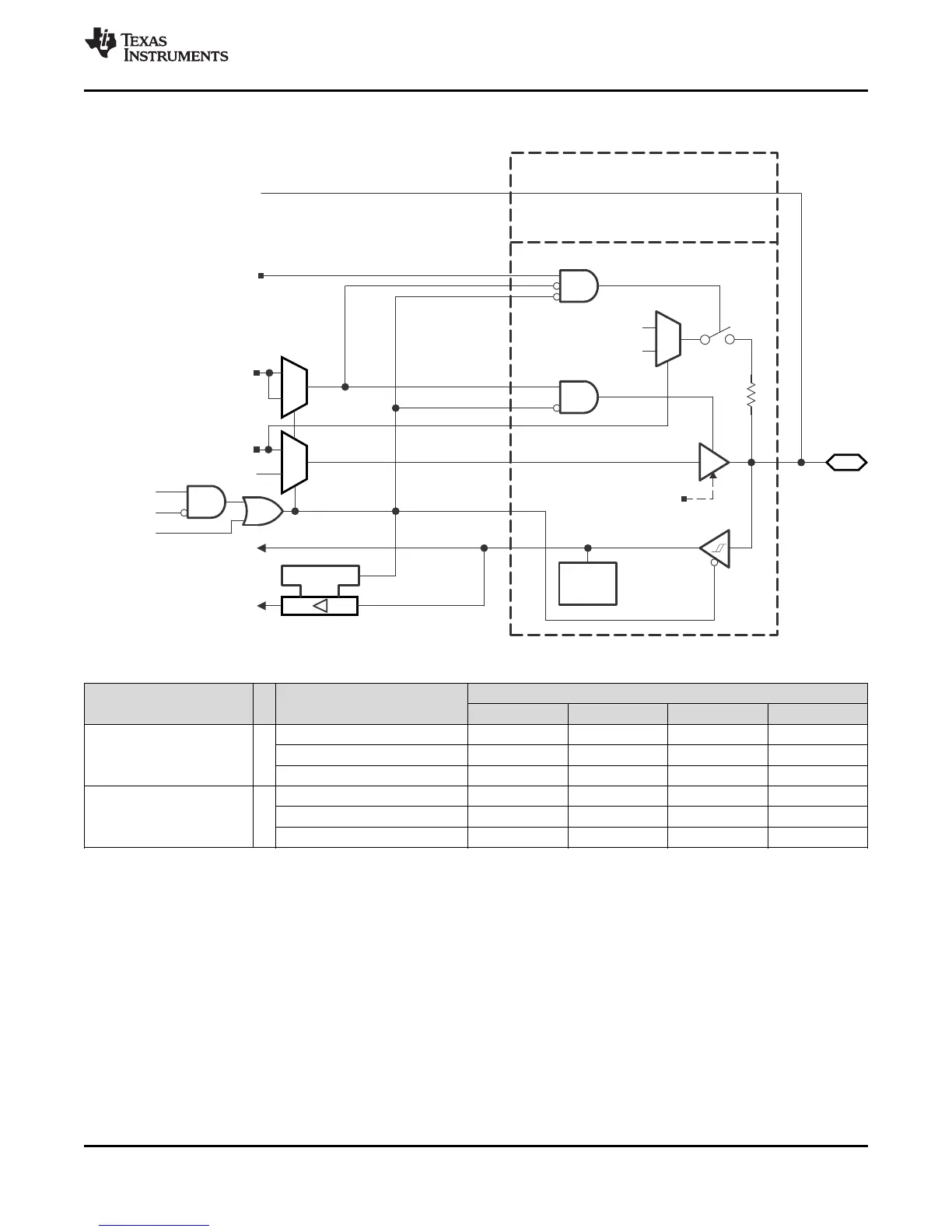
P5.3/XT2OUT
1
0
P5DIR.3
P5IN.3
EN
Module X IN
1
0
Module X OUT
P5OUT.3
1
0
DV
SS
DV
CC
P5REN.3
Pad Logic
1
P5DS.3
0: Low drive
1: High drive
D
Bus
Keeper
To XT2
P5SEL.2
XT2BYPASS
P5SEL.3
MSP430F5529
,
MSP430F5528
,
MSP430F5527
,
MSP430F5526
MSP430F5525
,
MSP430F5524
,
MSP430F5522
,
MSP430F5521
MSP430F5519, MSP430F5517, MSP430F5515, MSP430F5514, MSP430F5513
www.ti.com
SLAS590M –MARCH 2009–REVISED NOVEMBER 2015
6.10.7 Port P5, P5.3, Input/Output With Schmitt Trigger
Table 6-51. Port P5 (P5.2, P5.3) Pin Functions
CONTROL BITS OR SIGNALS
(1)
PIN NAME (P5.x) x FUNCTION
P5DIR.x P5SEL.2 P5SEL.3 XT2BYPASS
P5.2/XT2IN 2 P5.2 (I/O) I: 0; O: 1 0 X X
XT2IN crystal mode
(2)
X 1 X 0
XT2IN bypass mode
(2)
X 1 X 1
P5.3/XT2OUT 3 P5.3 (I/O) I: 0; O: 1 0 0 X
XT2OUT crystal mode
(3)
X 1 X 0
P5.3 (I/O)
(3)
X 1 0 1
(1) X = Don't care
(2) Setting P5SEL.2 causes the general-purpose I/O to be disabled. Pending the setting of XT2BYPASS, P5.2 is configured for crystal
mode or bypass mode.
(3) Setting P5SEL.2 causes the general-purpose I/O to be disabled in crystal mode. When using bypass mode, P5.3 can be used as
general-purpose I/O.
Copyright © 2009–2015, Texas Instruments Incorporated Detailed Description 89
Submit Documentation Feedback
Product Folder Links: MSP430F5529 MSP430F5528 MSP430F5527 MSP430F5526 MSP430F5525 MSP430F5524
MSP430F5522 MSP430F5521 MSP430F5519 MSP430F5517 MSP430F5515 MSP430F5514 MSP430F5513