www.ti.com
Magnetic Field Interface
3
SLOU410B–September 2015–Revised April 2020
Submit Documentation Feedback
Copyright © 2015–2020, Texas Instruments Incorporated
DRV425 Evaluation Module
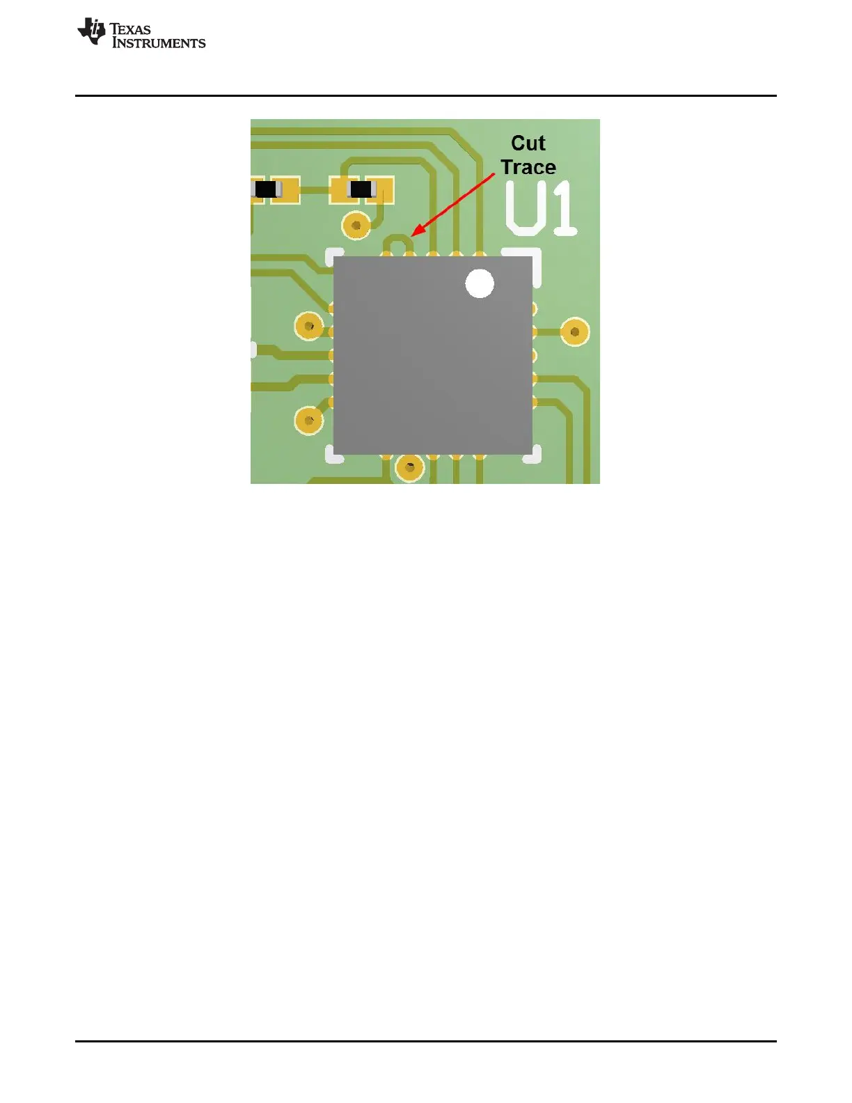
Figure 2. Board Modification for External Reference
An external reference can be applied to J1 pin 1, referenced to pin 3. If an external reference is used, it is
important to keep it at a level of VDD/2, which is the common mode point of the differential amplifier
output stage of the DRV425 device. Reference voltages beyond VDD/2 will result in offset and gain errors.
3.3 Output Voltage
The output voltage of the DRV425EVM is located on J1 pin 2 and can be referred to the reference at J1
pin 2 or the power supply ground at J1 pin 3.