OUT OUT
shunt
V V
B
G x Gfg x R 4 x 12.2 x R1
= =
EVM Operation
www.ti.com
4
SLOU410B–September 2015–Revised April 2020
Submit Documentation Feedback
Copyright © 2015–2020, Texas Instruments Incorporated
DRV425 Evaluation Module
4 EVM Operation
Factory setup of the DRV425EVM is for an input supply voltage range from 3.3 V to 5 V. Resistors R3
through R8 configure the reference voltage and bandwidth settings of the DRV425EVM. The default
conditions are listed in Table 2.
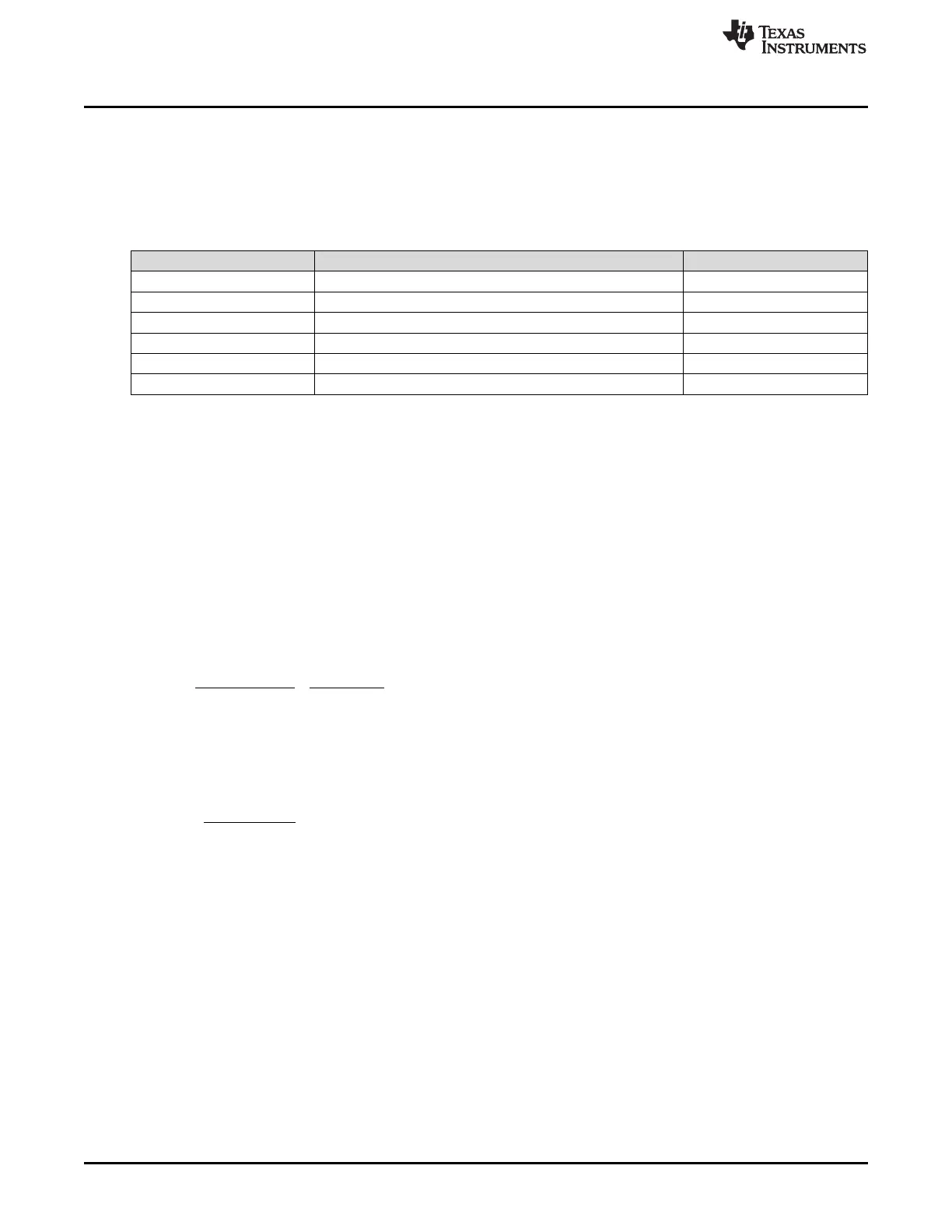
Table 2. Factory Configuration Defaults
RESISTOR FUNCTION DEFAULT CONDITION
R3 Pull-up for BSEL to VDD 0 Ω
R4 Pull-down for BSEL to GND open
R5 Pull-up for RSEL0 to VDD 0 Ω
R6 Pull-down for RSEL0 to GND open
R7 Pull-up for RSEL1 to VDD 0 Ω
R8 Pull-down for RSEL1 to GND open
If the default condition is not the desired configuration of the DRV425EVM, simply remove and replace the
resistors for the desired operating mode. If there is a desire to modify the state of the reference voltage or
device bandwidth during physical operation of the EVM, resistors R3 through R8 can be removed and
driven directly via GPIO pins on a microprocessor using fly wires.
4.1 Error and Over Range
R2 and R9 are 10-kΩ pull-up resistors on the Over Range (/OR) and Error (/ER) flag output pins
respectively. To observe the state of the flags, simply probe the chip side of the resistor. These outputs
are open drain and a pull up is required to observe the active low output state. These pins may also be fly-
wired to a micro controller for use as interrupt pins.
4.2 Calculation of Magnetic Field Strength
The magnetic field strength (B) can be calculated by Equation 1.
(1)
The maximum magnetic field range of the DRV425 is ±2 mT. With the 100 Ω shunt located at R1, the
maximum field measurement range is ±500 µT.To increase the sensitivity, R1 can be adjusted based on
Equation 1. Higher magnetic fields result in increased current flowing through R1. The output voltage of
the differential amplifier in the DRV425 will reach its peak amplitude with a maximum voltage drop across
R1 as shown in Equation 2.
(2)