MSP430F23x
MSP430F24x(1)
MSP430F2410
www.ti.com
SLAS547I –JUNE 2007–REVISED DECEMBER 2012
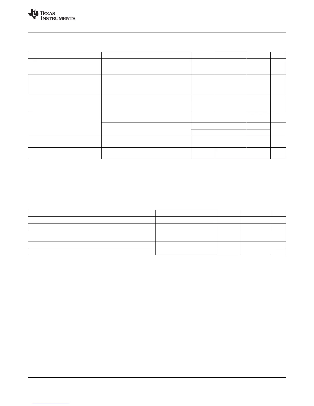
12-bit ADC, Power Supply and Input Range Conditions
(1)
over recommended operating free-air temperature range (unless otherwise noted)
PARAMETER TEST CONDITIONS V
CC
MIN TYP MAX UNIT
AV
CC
and DV
CC
are connected together
AV
CC
Analog supply voltage AV
SS
and DV
SS
are connected together 2.2 3.6 V
V
(AVSS)
= V
(DVSS)
= 0 V
All P6.0/A0 to P6.7/A7 terminals, Analog inputs
Analog input voltage selected in ADC12MCTLx register,
V
(P6.x/Ax)
0 V
AVCC
V
range
(2)
P6Sel.x = 1, 0 ≤ × ≤ 7,
V
(AVSS)
≤ V
P6.x/Ax
≤ V
(AVCC)
f
ADC12CLK
= 5 MHz, 2.2 V 0.65 0.8
Operating supply current
I
ADC12
ADC12ON = 1, REFON = 0, mA
into AV
CC
terminal
(3)
3 V 0.8 1
SHT0 = 0, SHT1 = 0, ADC12DIV = 0
f
ADC12CLK
= 5 MHz,
3 V 0.5 0.7 mA
ADC12ON = 0, REFON = 1, REF2_5V = 1
Operating supply current
I
REF+
into AV
CC
terminal
(4)
2.2 V 0.5 0.7
f
ADC12CLK
= 5 MHz,
mA
ADC12ON = 0, REFON = 1, REF2_5V = 0
3 V 0.5 0.7
Only one terminal can be selected at one time,
C
I
Input capacitance
(5)
2.2 V 40 pF
P6.x/Ax
Input MUX ON
R
I
0 V ≤ V
Ax
≤ V
AVCC
3 V 2000 Ω
resistance
(5)
(1) The leakage current is defined in the leakage current table with P6.x/Ax parameter.
(2) The analog input voltage range must be within the selected reference voltage range V
R+
to V
R–
for valid conversion results.
(3) The internal reference supply current is not included in current consumption parameter I
ADC12
.
(4) The internal reference current is supplied via terminal AV
CC
. Consumption is independent of the ADC12ON control bit, unless a
conversion is active. The REFON bit enables settling of the built-in reference before starting an A/D conversion.
(5) Not production tested, limits verified by design.
12-Bit ADC, External Reference
(1)
over recommended operating free-air temperature range (unless otherwise noted)
PARAMETER TEST CONDITIONS V
CC
MIN MAX UNIT
V
eREF+
Positive external reference voltage input V
eREF+
> V
REF–
/V
eREF–
(2)
1.4 V
AVCC
V
V
REF–
/V
eREF–
Negative external reference voltage input V
eREF+
> V
REF–
/V
eREF–
(3)
0 1.2 V
(V
eREF+
–
Differential external reference voltage input V
eREF+
> V
REF–
/V
eREF–
(4)
1.4 V
AVCC
V
V
REF–
/V
eREF–
)
I
VeREF+
Static leakage current 0 V ≤ V
eREF+
≤ V
AVCC
2.2 V, 3 V ±1 µA
I
VREF–/VeREF–
Static leakage current 0 V ≤ V
eREF–
≤ V
AVCC
2.2 V, 3 V ±1 µA
(1) The external reference is used during conversion to charge and discharge the capacitance array. The input capacitance, C
I
, is also the
dynamic load for an external reference during conversion. The dynamic impedance of the reference supply should follow the
recommendations on analog-source impedance to allow the charge to settle for 12-bit accuracy.
(2) The accuracy limits the minimum positive external reference voltage. Lower reference voltage levels may be applied with reduced
accuracy requirements.
(3) The accuracy limits the maximum negative external reference voltage. Higher reference voltage levels may be applied with reduced
accuracy requirements.
(4) The accuracy limits minimum external differential reference voltage. Lower differential reference voltage levels may be applied with
reduced accuracy requirements.
Copyright © 2007–2012, Texas Instruments Incorporated Submit Documentation Feedback 61

 Loading...


