www.SteamPoweredRadio.Com
5.3 AM Receiver Module Block Diagram Description
The
AM
Receiver module
is
tunable
from
540
to
1720
kHz
in
IO
kHz
steps. Audio output for external
use
is
balanced
600Q
at
up
to
+3
dBm.
Tuning
is via three rotary
DIP
switches which
are
accessible
by
removing the associated front panel cover plate.
An
LED lights to
show
RF signal presence and
audio output.
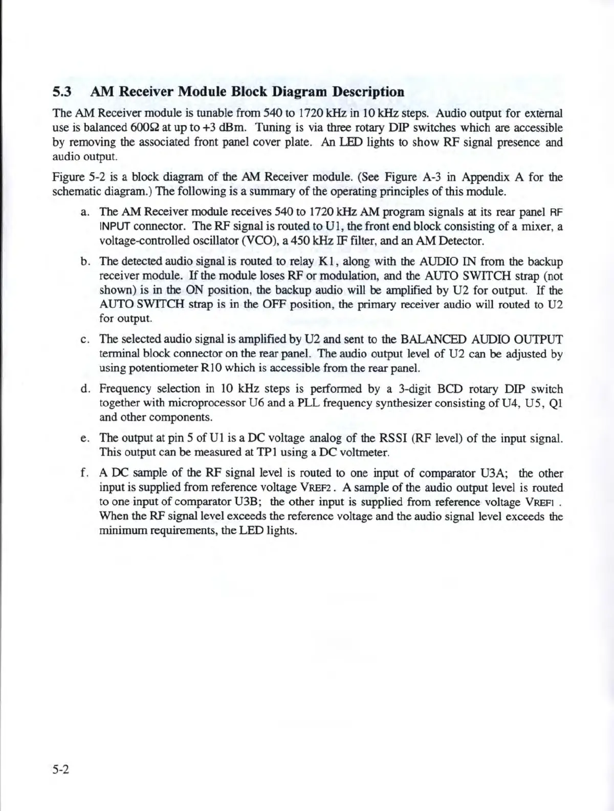
Fig
ur
e
5-2
is
a block diagram
of
the
AM
Receiver module. (
See
Figure
A-3 in Appendix A for the
schematic diagram.)
The
following is a summary
of
the operating principles
of
this module.
5-2
a.
The
AM
Receiver module receives
540
to 1720
kHz
AM
program signals
at
its rear panel
RF
INPUT connector.
The
RF signal
is
routed
to
Ul,
the front
end
block consisting
of
a
mixer
, a
vo
ltage-controlled oscillator (VCO), a
450
kHz
IF
filter, and
an
AM
Detector.
b.
The
detected a
udio
signal is routed to relay K 1, along with the AUDIO
IN
from the backup
receiver module.
If
the
module
lo
ses
RF
or
modulation, and the
AUTO
SWITCH
strap (not
s
hown
)
is
in the
ON
position, the backup audio will
be
amplified
by
U2
for output.
If
the
AUTO
SWITCH
strap is in the
OFF
position, the primary receiver audio will routed to
U2
for output.
c.
The
selected audio signal is amplified
by
U2
and
sent
to
the BALANCED AUDIO
OUTPUT
terminal block
co
nnector
on
the rear panel.
The
audio output level
of
U2
can
be adjusted by
using potentiometer R 10 which
is
accessible from the
rear
panel.
d . Frequency selection in
10
kH
.z steps is performed by a 3-digit
BCD
rotary
DIP
switch
together with microprocessor
U6
and
a
PLL
frequency synthesi
zer
consisting
of
U4,
U
5,
Ql
and
other
components.
e.
The
output
at
pin 5
of
Ul
is
a
DC
voltage analog
of
the
RSSI
(RF level)
of
the input signal.
This
output
can
be
measured
at
TP 1 using a
DC
vo
ltmeter.
f.
A DC samp
le
of
the
RF
signal level is routed to
one
input
of
comparator U3A; the other
input is supplied
from
reference voltage
VREF2
. A samp
le
of
the audio output level
is
routed
to
one
input
of
comparator
U3B
; the
other
input is supplied from reference voltage
VREFJ
.
When
the RF signal level exceeds the reference voltage
and
the audio signal level exceeds the
minimum requirements, the
LED
lights.