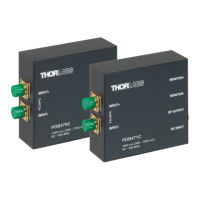
Si Biased Detector
Page 13 Rev F, December 8, 2014
Chapter 7 Specifications
All measurements performed with a 50 Ω load unless stated otherwise.
Electrical Specifications
Detector Si PIN
Active Area Ø9.8 mm (75.4 mm
2
)
Wavelength Range λ 400 to 1100 nm
Peak Wavelength λ
p
970 nm
Peak Response
2
ℜ( λ
p
)
0.65 A/W
Shunt Resistance R
sh
1 GΩ
Diode Capacitance C
J
300 pF
Rise Time
2,3
t
r
43 ns
NEP (λ
p
) 2.07 x 10
-13
W/√Hz
Bias Voltage V
R
10 V
Dark Current
2
(with 1 MΩ Load) I
D
100 nA (Typ)
600 nA (Max)
Output Voltage V
OUT
0 to 10 V
General
On/Off Switch Slide
Battery Check Switch Momentary Pushbutton
Output BNC (DC Coupled)
Package Size 2.8" x 1.9" x 0.83"
(70 mm x 48 mm x 21 mm)
PD Surface Depth 0.13" (3.4 mm)
Weight 0.2 kg
Accessories SM1T1 Coupler
SM1RR Retainer Ring
Storage Temp -20 to 70 °C
Operating Temp 10 to 50 °C
Battery A23, 12 V
DC
, 40 mAh
Low Battery Voltage
4
(See Battery Check)
V
OUT
(Hi-Z) ~9 V
V
OUT
(50Ω) ~400 mV
2
Measured with specified bias voltage of 10.0 V
3
Low battery voltage will result in slower rise times and decreased bandwidth.
4
Assumes the battery voltage drops below 9.6 V. The reverse protection diode generates a 0.6 V drop.