Page 12
MTN003813_D02
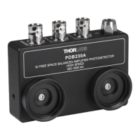
PDB2xx Series
5 Appendix
5 Appendix
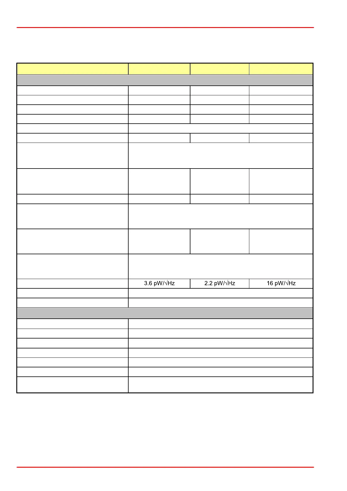
5.1 Technical Data
Diameter of Active Detector Area
RF OUTPUT Bandwidth (3dB)
Common Mode Rejection Ratio (Typ.)
RF OUTPUT Transimpedance Gain
High Z load
50 W load
500 x 10
3
V/A
175 x 10
3
V/A
RF OUTPUT Conversion Gain
High Z load
50 W load
250 x 10
3
V/W
85 x 10
3
V/W
300 x 10
3
V/W
100 x 10
3
V/W
500 x 10
3
V/W
175 x 10
3
V/W
RF OUTPUT CW Saturation Power
RF OUTPUT Voltage Swing
High Z load
50 W load
MONITOR Output Conversion Gain
High Z load
50 W load
MONITOR Output Voltage Swing
High Z load
50 W load
Photo Diode Damage Threshold
DC (AC coupling on request)
Operating Temperature Range
1
)
Storage Temperature Range
83.8 mm x 65.3 mm x 21.1 mm (3.30" x 2.57" x 0.83")
0.15 kg (w/o power supply)
± 12 V @ 250 mA
(100/120/230 VAC, 50-60 Hz, Switchable)
1
) non-condensing
All technical data are valid at 23 ± 5°C and 45 ± 15% rel. humidity (non condensing)