SARA-G3 series - System Integration Manual
UBX-13000995 - R06 Objective Specification Design-in
Page 123 of 218
Limit capacitance and series resistance on each SIM signal (SIM_CLK, SIM_IO, SIM_RST) to match
the requirements for the SIM interface (27.7 ns is the maximum allowed rise time on the SIM_CLK
line, 1.0 µs is the maximum allowed rise time on the SIM_IO and SIM_RST lines)
SARA-G3 series
41
VSIM
39
SIM_IO
38
SIM_CLK
40
SIM_RST
4
V_INT
42
SIM_DET
SIM CARD
HOLDER
C
5
C
6
C
7
C
1
C
2
C
3
SIM Card
Bottom View
(contacts side)
C1
VPP (C6)
VCC (C1)
IO (C7)
CLK (C3)
RST (C2)
GND (C5)
C2 C3 C5
J1
C4
D1 D2 D3 D4
C
8
C
4
TP
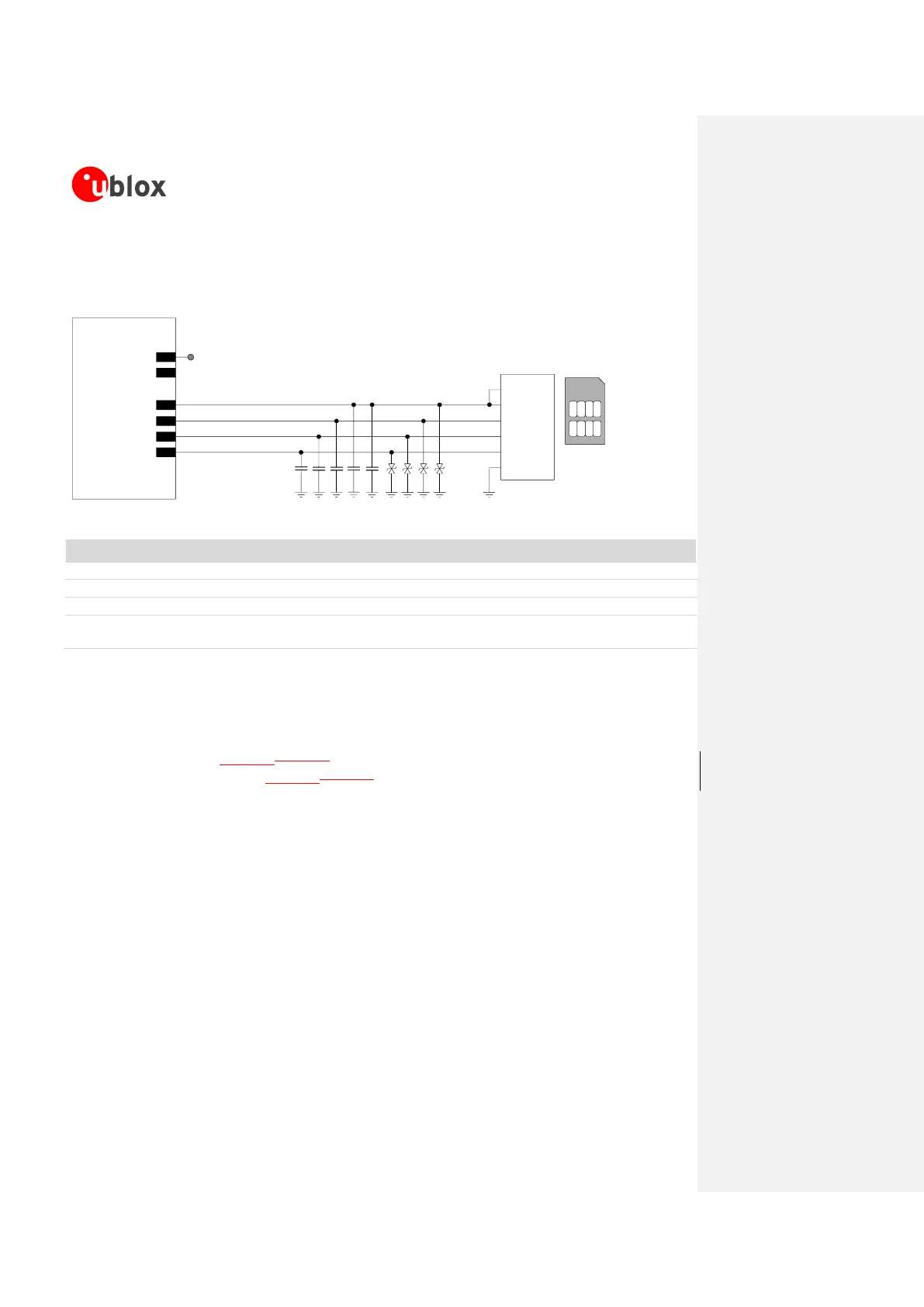
Figure 43: Application circuit for the connection to a single removable SIM card, with SIM detection not implemented
Part Number - Manufacturer
47 pF Capacitor Ceramic C0G 0402 5% 50 V
GRM1555C1H470JA01 - Murata
100 nF Capacitor Ceramic X7R 0402 10% 16 V
GRM155R71C104KA01 - Murata
Very Low Capacitance ESD Protection
PESD0402-140 - Tyco Electronics
SIM Card Holder
6 positions, without card presence switch
Various Manufacturers,
C707 10M006 136 2 - Amphenol
Table 23: Example of components for the connection to a single removable SIM card, with SIM detection not implemented
Guidelines for single SIM chip connection
A solderable SIM chip (M2M UICC Form Factor) must be connected the SIM card interface of SARA-G3
modules as described in Figure 44Figure 44, where the optional SIM detection feature is not implemented
(refer to the circuit described in Figure 45Figure 45 if the SIM detection feature is not required).
Follow these guidelines connecting the module to a solderable SIM chip without SIM presence detection:
Connect the UICC / SIM contacts C1 (VCC) and C6 (VPP) to the VSIM pin of the module
Connect the UICC / SIM contact C7 (I/O) to the SIM_IO pin of the module
Connect the UICC / SIM contact C3 (CLK) to the SIM_CLK pin of the module
Connect the UICC / SIM contact C2 (RST) to the SIM_RST pin of the module
Connect the UICC / SIM contact C5 (GND) to ground
Provide a 100 nF bypass capacitor (e.g. Murata GRM155R71C104K) at the SIM supply line (VSIM)
close to the relevant pad of the SIM chip, to prevent digital noise
Provide a bypass capacitor of about 22 pF to 47 pF (e.g. Murata GRM1555C1H470J) on each SIM
line (VSIM, SIM_CLK, SIM_IO, SIM_RST), to prevent RF coupling especially in case the RF
antenna is placed closer than 10 - 30 cm from the SIM card holder
Limit capacitance and series resistance on each SIM signal (SIM_CLK, SIM_IO, SIM_RST) to match
the requirements for the SIM interface (27.7 ns is the maximum allowed rise time on the SIM_CLK
line, 1.0 µs is the maximum allowed rise time on the SIM_IO and SIM_RST lines)
 Loading...