SARA-G3 series - System Integration Manual
UBX-13000995 - R06 Objective Specification Design-in
Page 137 of 218
“GNSS data ready” and “GNSS RTC sharing” functions are not supported by all u-blox GNSS
receivers HW or ROM/FW versions. Refer to the
GNSS Implementation Application Note
[21] or to
the
Hardware Integration Manual
of the u-blox GNSS receivers for the supported features.
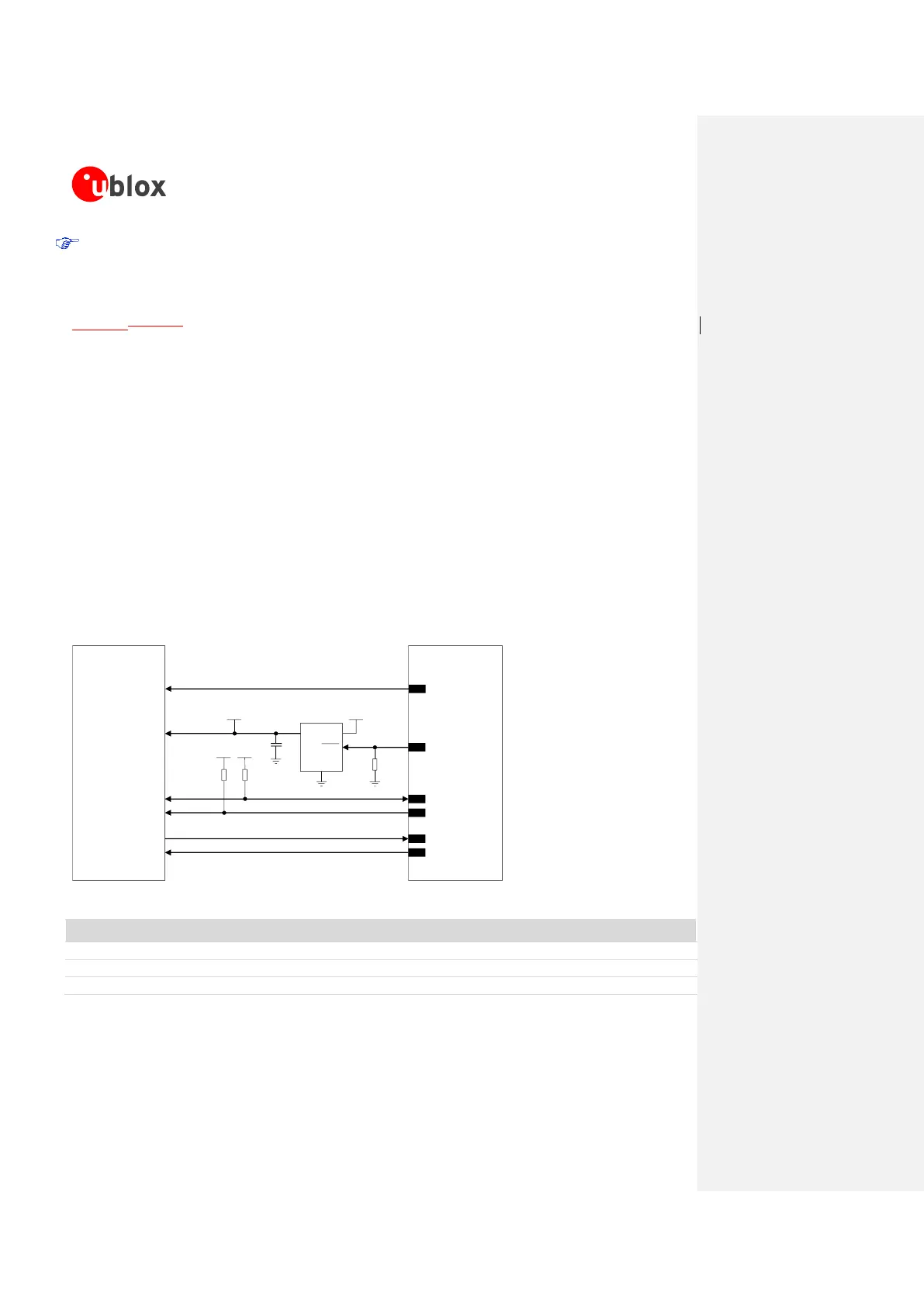
Figure 55Figure 55 illustrates an application circuit for SARA-G350 connection to a u-blox 1.8 V GNSS
receiver:
The SDA and SCL pins of the SARA-G350 module are directly connected to the related pins of the
u-blox 1.8 V GNSS receiver, with appropriate pull-up resistors.
The GPIO3 and GPIO4 pins are directly connected respectively to TXD1 and EXTINT0 pins of the u-
blox 1.8 V GNSS receiver providing “GNSS data ready” and “GNSS RTC sharing” functions.
The GPIO2 pin is connected to the active-high enable pin of the voltage regulator that supplies the
u-blox 1.8 V GNSS receiver providing the “GNSS supply enable” function. A pull-down resistor is
provided to avoid a switch on of the positioning receiver when the SARA-G350 module is switched off
or in the reset state.
The V_BCKP supply output of the SARA-G350 wireless module is connected to the V_BCKP backup
supply input pin of the GNSS receiver to provide the supply for the GNSS real time clock and backup
RAM when the VCC supply of the wireless module is within its operating range and the VCC supply
of the GNSS receiver is disabled. This enables the u-blox GNSS receiver to recover from a power
breakdown with either a Hot-start or a Warm-start (depending on the actual duration of the GNSS
VCC outage) and to maintain the configuration settings saved in the backup RAM.
SARA-G350
R1
INOUT
GND
GNSS LDO
Regulator
SHDN
u-blox GNSS
1.8 V receiver
SDA2
SCL2
R2
1V8 1V8
VMAIN1V8
U1
23
GPIO2
SDA
SCL
C1
TxD1
EXTINT0
GPIO3
GPIO4
26
27
24
25
VCC
R3
V_BCKP V_BCKP
2
Figure 55: DDC (I
2
C) application circuit for u-blox 1.8 V GNSS receiver
Part Number - Manufacturer
4.7 kΩ Resistor 0402 5% 0.1 W
RC0402JR-074K7L - Yageo Phycomp
47 kΩ Resistor 0402 5% 0.1 W
RC0402JR-0747KL - Yageo Phycomp
Voltage Regulator for GNSS receiver
See GNSS receiver Hardware Integration Manual
Table 31: Components for DDC (I
2
C) application circuit for u-blox 1.8 V GNSS receiver
 Loading...