SARA-G3 series - System Integration Manual
UBX-13000995 - R06 Objective Specification Design-in
Page 94 of 218
kHz must be carefully evaluated since this can produce noise in the VCC voltage profile and therefore
negatively impact GSM modulation spectrum performance. An additional L-C low-pass filter between the
switching regulator output to VCC supply pins can mitigate the ripple on VCC, but adds extra voltage
drop due to resistive losses on series inductors
PWM mode operation: it is preferable to select regulators with Pulse Width Modulation (PWM) mode.
While in connected-mode Pulse Frequency Modulation (PFM) mode and PFM/PWM mode, transitions
must be avoided to reduce the noise on the VCC voltage profile. Switching regulators that are able to
switch between low ripple PWM mode and high efficiency burst or PFM mode can be used, provided
the mode transition occurs when the module changes status from idle/active-mode to connected-mode
(where current consumption increases to a value greater than 100 mA): it is permissible to use a
regulator that switches from the PWM mode to the burst or PFM mode at an appropriate current
threshold (e.g. 60 mA)
Output voltage slope: the use of the soft start function provided by some voltage regulators should be
carefully evaluated, since the VCC pins voltage must ramp from 2.5 V to 3.2 V within 4 ms to
switch on the module that otherwise can be switched on by a low level on PWR_ON pin
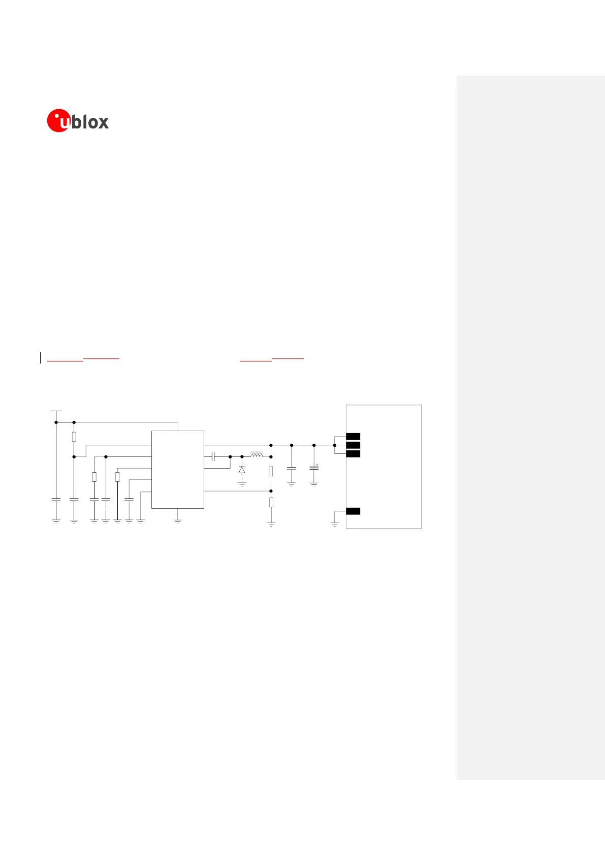
Figure 27Figure 27 and the components listed in Table 13Table 13 show an example of a high reliability
power supply circuit, where the module VCC is supplied by a step-down switching regulator capable of
delivering 1.9 A current pulses with low output ripple and with fixed switching frequency in PWM mode
operation greater than 1 MHz.
SARA-G3 series
12V
C5
R3
C4
R2
C2C1
R1
VIN
RUN
VC
RT
PG
SYNC
BD
BOOST
SW
FB
GND
6
7
10
9
5
C6
1
2
3
8
11
4
C7 C8
D1
R4
R5
L1
C3
U1
52
VCC
53
VCC
51
VCC
GND
Figure 27: Suggested schematic design for the VCC voltage supply application circuit using a step-down regulator
 Loading...