SARA-G3 series - System Integration Manual
UBX-13000995 - R06 Objective Specification Design-in
Page 96 of 218
Part Number - Manufacturer
5.2 µH Inductor 30% 5.28A 22 m
MSS1038-522NL – Coilcraft
4.7 k Resistor 0402 1% 0.063 W
910 Resistor 0402 1% 0.063 W
82 Resistor 0402 5% 0.063 W
8.2 k Resistor 0402 5% 0.063 W
39 k Resistor 0402 5% 0.063 W
Step-Down Regulator 8-VFQFPN 3 A 1 MHz
L5987TR – ST Microelectronics
Table 14: Suggested components for low cost solution VCC voltage supply application circuit using a step-down regulator
2.1.1.3 Guidelines for VCC supply circuit design using a Low Drop-Out (LDO) linear regulator
The use of a linear regulator is suggested when the difference from the available supply rail and the VCC
value is low: linear regulators provide high efficiency when transforming a 5 V supply to a voltage value
within the module VCC normal operating range.
The characteristics of the LDO linear regulator connected to the VCC pins should meet the following
prerequisites to comply with the module VCC requirements summarized in Table 6Table 6:
Power capabilities: the LDO linear regulator with its output circuit must be capable of providing a
proper voltage value to the VCC pins and of delivering 1.9 A current pulses with 1/8 duty cycle
Power dissipation: the power handling capability of the LDO linear regulator must be checked to limit
its junction temperature to the maximum rated operating range (i.e. check the voltage drop from the
max input voltage to the min output voltage to evaluate the power dissipation of the regulator)
Output voltage slope: the use of the soft start function provided by some voltage regulator should be
carefully evaluated, since the VCC pins voltage must ramp from 2.5 V to 3.2 V within 4 ms to
switch-on the module that otherwise can be switched on by a low level on PWR_ON pin
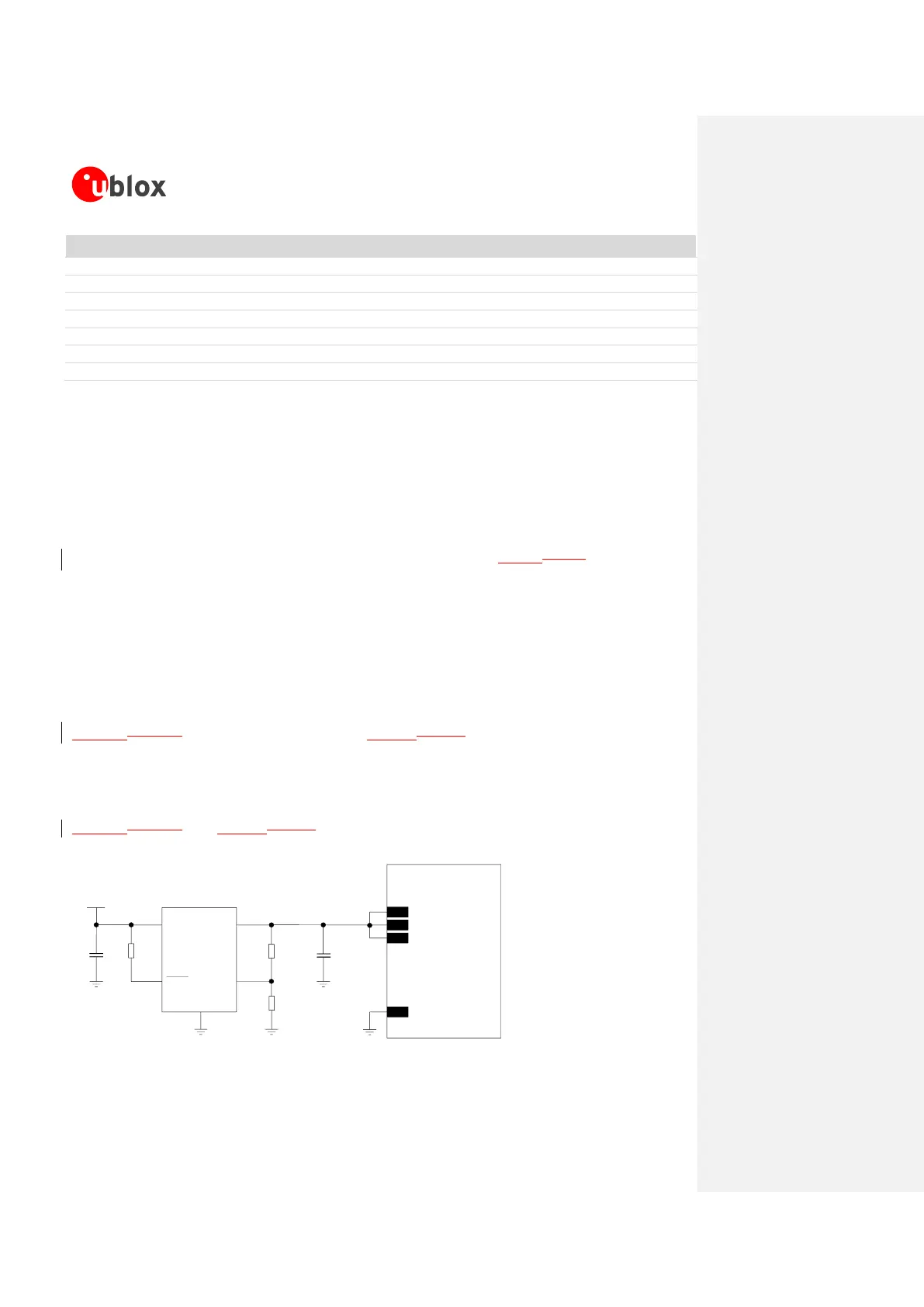
Figure 29Figure 29 and the components listed in Table 15Table 15 show an example of a power supply
circuit, where the VCC module supply is provided by an LDO linear regulator capable of delivering 1.9 A
current pulses, with proper power handling capability.
It is recommended to configure the LDO linear regulator to generate a voltage supply value slightly below
the maximum limit of the module VCC normal operating range (e.g. ~4.1 V as in the circuit described in
Figure 29Figure 29 and Table 15Table 15). This reduces the power on the linear regulator and improves
the thermal design of the supply circuit.
5V
C1 R1
IN OUT
ADJ
GND
1
2
4
5
3
C2R2
R3
U1
SHDN
SARA-G3 series
52
VCC
53
VCC
51
VCC
GND
Figure 29: Suggested schematic design for the VCC voltage supply application circuit using an LDO linear regulator
 Loading...