SARA-G3 series - System Integration Manual
UBX-13000995 - R06 Objective Specification Design-in
Page 98 of 218
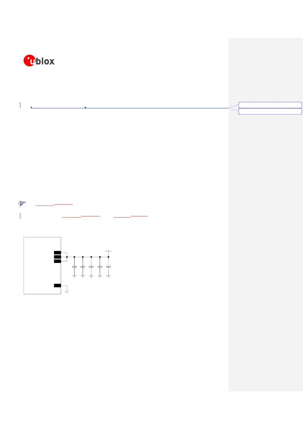
To avoid voltage drop undershoot and overshoot at the start and end of a transmit burst during a GSM
call (when current consumption on the VCC supply can rise up to 1.9 A in the worst case), place a
bypass capacitor with large capacitance (more than 100 µF) and low ESR near the VCC pins, for
example:
330 µF capacitance, 45 m ESR (e.g. KEMET T520D337M006ATE045, Tantalum Capacitor)
The use of very large capacitors (i.e. greater then 1000 µF) on the VCC line should be carefully
evaluated, since the voltage at the VCC pins must ramp from 2.5 V to 3.2 V within 4 ms to switch on
the module that otherwise can be switched on by a low level on PWR_ON pin.
To reduce voltage ripple and noise, especially if the application device integrates an internal antenna, place
the following bypass capacitors near the VCC pins:
100 nF capacitor (e.g Murata GRM155R61C104K) to filter digital logic noise from clocks and data
sources
10 nF capacitor (e.g. Murata GRM155R71C103K) to filter digital logic noise from clocks and data
sources
56 pF capacitor with Self-Resonant Frequency in 800/900 MHz range (e.g. Murata
GRM1555C1E560J) to filter transmission EMI in the GSM/EGSM bands
15 pF capacitor with Self-Resonant Frequency in 1800/1900 MHz range (e.g. Murata
GRM1555C1E150J) to filter transmission EMI in the DCS/PCS bands
Figure 30Figure 30 shows the complete configuration but the mounting of each single component
depends on the application design: it is recommended to provide all the VCC bypass capacitors as
described in Figure 30Figure 30 and Table 16Table 16 if the application device integrates an
internal antenna.
C4
GND
C3 C2
SARA-G3 series
52
VCC
53
VCC
51
VCC
3V8
C1
+
C5
Figure 30: Suggested schematic and layout design for the VCC bypass capacitors to reduce ripple / noise on VCC voltage profile and to
avoid undershoot / overshoot on VCC voltage drops
Formatted: French (France)
Formatted: French (France)
 Loading...