NINA-W1 series - System integration manual
UBX-17005730 - R11 Design-in Page 38 of 55
C1 - Public
• Proper placement of the antenna and its surroundings is also critical for antenna performance.
Avoid placing the antenna close to conductive or RF-absorbing parts such as metal objects, ferrite
sheets and so on as they may absorb part of the radiated power or shift the resonant frequency of
the antenna or affect the antenna radiation pattern.
• It is highly recommended to strictly follow the detailed and specific guidelines provided by the
antenna manufacturer regarding correct installation and deployment of the antenna system,
including PCB layout and matching circuitry.
• Further to the custom PCB and product restrictions, antennas may require tuning/matching to
comply with all the applicable required certification schemes. It is recommended to consult the
antenna manufacturer for the design-in guidelines and plan the validation activities on the final
prototypes like tuning/matching and performance measures. See also Table 3.
• RF section may be affected by noise sources like hi-speed digital buses. Avoid placing the antenna
close to buses such as DDR or consider taking specific countermeasures like metal shields or
ferrite sheets to reduce the interference.
⚠ Take care of the interaction between co-located RF systems like LTE sidebands on 2.4 GHz band.
Transmitted power may interact or disturb the performance of NINA-W1 modules.
3.3.3 On-board antenna design
If a plastic enclosure is used, it is possible to use NINA-W1 with the embedded antenna. In order to
reach an optimum operating performance, follow the instructions provided in the sections below.
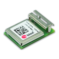
3.3.3.1 NINA-W1x2 – Internal PIFA antenna
• The module shall be placed in the corner of the host PCB with the antennas feed point in the corner
(pins 15 and 16), as shown in Figure 27. Other edge placements positions, with the antenna
closest to the edge, are also possible. However, these placements give only a moderately reduced
antenna performance compared to a corner placement.
• A large ground plane on the host PCB is a prerequisite for good antenna performance.
• The host PCB shall include a full GND plane underneath the entire module, including the antenna
section. This to facilitate efficient grounding of the module.
• High / large parts including metal shall not be placed closer than 10 mm to the module’s antenna.
• At least 5 mm clearance between the antenna and the casing is needed. If the clearance is less
than 5 mm, the antenna performance will be affected. PC and ABS gives less impact and POS type
plastic gives more.
• The module shall be placed such that the antenna faces outwards from the product and is not
obstructed by any external items in close vicinity of the products intended use case.
Figure 27: Placement of NINA-W1x2 with internal PIFA antenna
 Loading...